A Gaussian metal-semiconductor resonator for nanolasers

A metal semiconductor and nano-laser technology, applied in the structure of optical resonators, lasers, laser components, etc., can solve the problems of large laser threshold current, difficult lasing, large surface plasmon loss, etc., and achieve a lower threshold current, easy to manufacture, and the effect of reducing metal loss

Active Publication Date: 2020-07-24
NANJING UNIV OF SCI & TECH
View PDF5 Cites 0 Cited by
  • Summary
  • Abstract
  • Description
  • Claims
  • Application Information

AI Technical Summary

Problems solved by technology

[0003] At present, researchers have proposed many metal-semiconductor resonators with different structures, but the traditional rectangular metal-semiconductor resonators have large surface plasmon losses, and the threshold current required to excite the laser is very large, making it difficult to achieve lasing.

Method used


Image

  • A Gaussian metal-semiconductor resonator for nanolasers
  • A Gaussian metal-semiconductor resonator for nanolasers
  • A Gaussian metal-semiconductor resonator for nanolasers

Examples


Embodiment

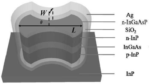
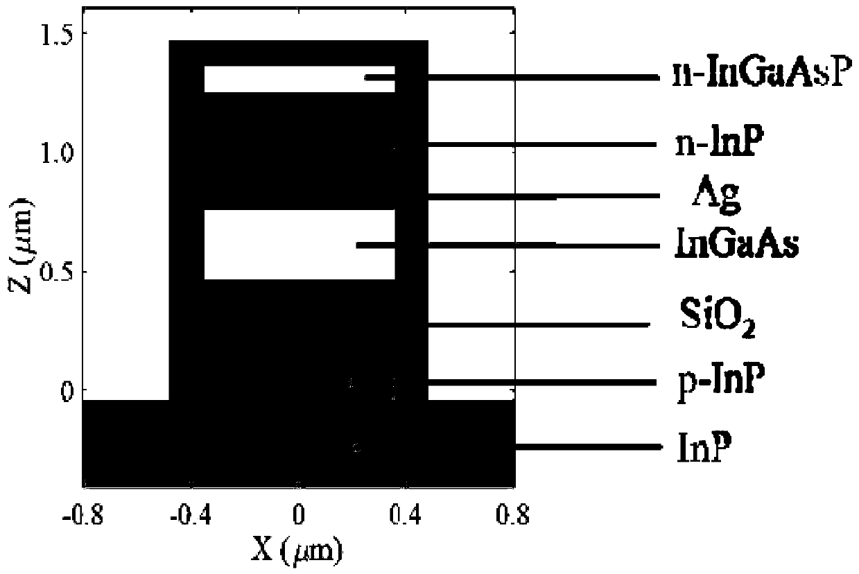
[0021] Such as figure 1 , figure 2 As shown, a Gaussian metal-semiconductor resonator for nano-lasers, the metal-semiconductor resonator is a Gaussian beam-type structure, the reflective surface of the structure has a curvature of 0.6-1.5 times the cavity length, and the side wall has a Gaussian cavity length dimension beam configuration.

[0022] The metal-semiconductor resonant cavity is composed of metal, insulator and semiconductor material from the outside to the inside; the reflective surface and the curved side wall can effectively reduce the metal surface plasmon loss. The dimensions of the resonant cavity are on the sub-wavelength level.

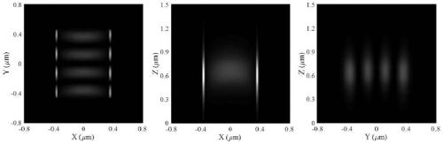
[0023] The lasing mode of the Gaussian metal-semiconductor resonator used in the nanolaser is the Fabry-Perot mode.

[0024] Metal shells are used as current injection electrodes in semiconductor photonic integrated circuits (PICs).

[0025] The hyperbolic shape of the sidewall of the metal-semiconductor resonator and the curva...


PUM

PropertyMeasurementUnit
thicknessaaaaaaaaaa
thicknessaaaaaaaaaa
thicknessaaaaaaaaaa

Abstract

The invention discloses a Gaussian-type metal semiconductor resonant cavity for a nano laser. The resonant cavity is a double-concave semiconductor resonant cavity composed of a semiconductor materialcovered witha metal shell layer, and has a resonant cavity structure in the shape of a Gaussian beam. The invention provides a novel Gaussian-type resonant cavity structure to reduce the surface plasmon loss of a metal semiconductor cavity. The circular arc-shaped reflecting surface of the resonant cavity can concentrate the resonant mode at the center of the cavity, so that the field distribution of the resonant mode is far away from the metal sidewall, thereby effectively reducing the metal loss. The electric field component perpendicular to the metal sidewall can be reduced by the curvedsidewall of the resonator, which can further suppress the surface plasmon loss. Reasonable design of reflection surface and curved sidewall of the resonator reflector can effectively reduce the threshold current of excitation resonator, and provide technical reference for the resonator design of nano-laser and related fields such as photonic integrated circuit, optical interconnection and so on.

Description

technical field [0001] The invention belongs to the field of semiconductor lasers, in particular to a Gaussian metal semiconductor resonant cavity used for nanometer lasers. Background technique [0002] Metal semiconductor lasers are widely used in semiconductor photonic integrated circuits, optical communications and other fields due to their small size and low excitation energy. [0003] At present, researchers have proposed many metal-semiconductor resonators with different structures, but the traditional rectangular metal-semiconductor resonators have large surface plasmon losses, and the threshold current required to excite the laser is very large, making it difficult to achieve lasing. . Contents of the invention [0004] The object of the present invention is to provide a Gaussian metal-semiconductor resonant cavity used for a nano-laser, and improve the energy excitation efficiency of the metal-semiconductor resonant cavity. [0005] The technical solution for r...

Claims


Application Information

Patent Timeline
Patent Type & Authority Patents(China)
IPC IPC(8): H01S5/10H01S5/32H01S5/323
CPCH01S5/10H01S5/1039H01S5/32H01S5/323
Inventor 张柏富朱康武恒胡海峰
Owner NANJING UNIV OF SCI & TECH
Why Eureka
Try Eureka