
A method of conductive embolism and semiconductor device with conductive embolism

A conductive plug and semiconductor technology, which is applied in the direction of semiconductor devices, semiconductor/solid device manufacturing, semiconductor/solid device components, etc., can solve the problems of metal tungsten stripping, high resistance of tungsten plugs, affecting device reliability, etc., to eliminate gaps formation, void volume reduction, and high reliability

Active Publication Date: 2021-03-30
CHANGXIN MEMORY TECH INC
View PDF12 Cites 0 Cited by
  • Summary
  • Abstract
  • Description
  • Claims
  • Application Information

AI Technical Summary

Problems solved by technology

However, metal tungsten is deposited by chemical vapor deposition method CVD on a silicon wafer or silicon glass with a contact hole opening. As the process of filling the contact hole opening with metal tungsten continues, due to the relatively fast deposition rate of metal tungsten on the upper part of the contact hole, Before the entire contact hole opening is completely filled, the opening has been sealed in advance, resulting in void defects in the formed tungsten plug, which affects the reliability of the device
In the subsequent chemical mechanical polishing CMP or etching process to remove excess tungsten metal, the voids in the tungsten plug are exposed, or after the CMP process, due to the reaction of the reactant and the metal tungsten in the contact hole, the metal tungsten is removed from the contact hole. Stripping in the contact hole, causing loss of tungsten
In the prior art, the generation of voids can be reduced by reducing the temperature, adjusting the pressure and gas flow and other parameters during the CVD process, but the resistance of the tungsten plug deposited in such an environment is too high, which is not conducive to the conduction between the metal layers

Method used

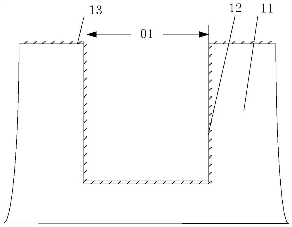
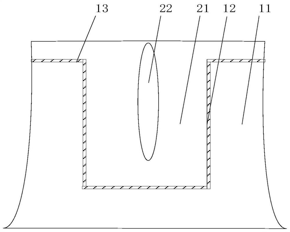

Image

  • A method of conductive embolism and semiconductor device with conductive embolism
  • A method of conductive embolism and semiconductor device with conductive embolism
  • A method of conductive embolism and semiconductor device with conductive embolism

Examples


Embodiment Construction

[0053] In the following, only some exemplary embodiments are briefly described. As those skilled in the art would realize, the described embodiments may be modified in various different ways, all without departing from the spirit or scope of the present invention. Accordingly, the drawings and descriptions are to be regarded as illustrative in nature and not restrictive.

[0054] In describing the present invention, it is to be understood that the terms "center", "longitudinal", "transverse", "length", "width", "thickness", "upper", "lower", "front", " Back", "Left", "Right", "Straight", "Horizontal", "Top", "Bottom", "Inner", "Outer", "Clockwise", "Counterclockwise", etc. or The positional relationship is based on the orientation or positional relationship shown in the drawings, which are only for the convenience of describing the present invention and simplifying the description, rather than indicating or implying that the referred device or element must have a specific ori...


PUM

PropertyMeasurementUnit
pore sizeaaaaaaaaaa
depthaaaaaaaaaa
thicknessaaaaaaaaaa

Abstract

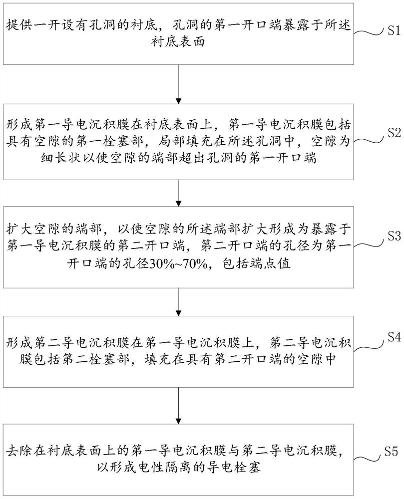
The invention discloses a preparation method of a conductive plug, comprising the steps of: providing a substrate with a hole, wherein a first open end of the hole is exposed to the surface of the substrate; forming a first conductive deposition film on the surface of the substrate, the first conductive deposition film including a first plug portion having a void partially filled in the void, thevoid being elongated such that the end of the void extends beyond the first open end of the void; enlarging an end portion of the void such that the end portion of the void is enlarged to be exposed to a second open end of the first conductive deposition film, the aperture of the second open end being 30% to 70% of the aperture of the first open end, including an endpoint value; forming a second conductive deposition film on the first conductive deposition film, the second conductive deposition film including a second plug portion filled in a gap having a second open end; and removing the first conductive deposition film and the second conductive deposition film on the surface of the substrate to form electrically isolated conductive plugs. The method reduces the volume of the voids or eliminates the voids so as to obtain a conductive plug with low resistance and high reliability.

Description

technical field [0001] The invention belongs to the technical field of semiconductor manufacturing, and in particular relates to a method for preparing a conductive plug and a semiconductor device with a conductive plug. Background technique [0002] In the manufacture of semiconductor chips, the integration level of VLSI chips has reached hundreds of millions or even billions of devices, which makes the application of more than two layers of multilayer metal interconnection technology more important. At present, the electrical connection between two different metal layers can be realized by forming a plug structure between the two metal layers. The quality of the plug formation has a great influence on the performance of the device. If the quality of the plug formation is poor, it will make the interconnection The resistance increases, affecting the performance of the device. [0003] Metal tungsten is the preferred material for plugs due to its excellent step coverage and...

Claims


Application Information

Patent Timeline
Patent Type & Authority Patents(China)
IPC IPC(8): H01L21/768H01L23/532
CPCH01L21/76882H01L21/76883H01L23/53266
Inventor 不公告发明人
Owner CHANGXIN MEMORY TECH INC
Learn More