

OTFT ammonia gas sensor embedded with small molecule additive and preparation method of OTFT ammonia gas sensor
A technology of ammonia sensor and additive, which is applied in semiconductor/solid-state device manufacturing, electrical components, electric solid-state devices, etc., can solve problems such as poor stability, achieve good stability, improve stability, and be easy to implement and promote.
- Summary
- Abstract
- Description
- Claims
- Application Information
AI Technical Summary
Problems solved by technology
Method used
Image

Examples
Embodiment 1
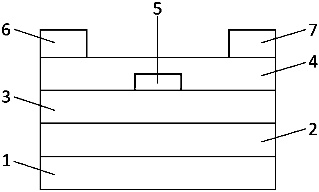
[0057] Embodiment 1: A kind of OTFT ammonia gas sensor embedded with small molecule additive provided by the preferred embodiment of the present invention, such as figure 1 As shown, it is a bottom-gate top-contact structure, and the material and thickness of each layer of the device are: substrate 1 is glass; gate electrode 2 is ITO, with a thickness of 200nm; dielectric layer 3 is PMMA, with a thickness of 500nm; organic semiconductor layer 4 is P3HT with a thickness of 30nm; the embedded small molecule additive 5 is TCNQ; the source electrode 6 and the drain electrode 7 are both Au with a thickness of 50nm.
[0058] The preparation method is as follows:
[0059] 1. Thoroughly clean the substrate 1 on which the gate electrode ITO has been sputtered, and dry it with dry nitrogen after cleaning;
[0060] 2. Prepare a PMMA film on the surface of ITO by spin coating to form a dielectric layer 3;
[0061] 3. Heat and bake the spin-coated PMMA film to remove excess solvent;
[...
Embodiment 2
[0065] Embodiment 2: A kind of OTFT ammonia gas sensor embedded with small molecule additive provided by the preferred embodiment of the present invention, such as figure 1 The bottom-gate top-contact structure is shown, and the material and thickness of each layer of the device are as follows: substrate 1 is polytetrafluoroethylene; gate electrode 2 is ITO with a thickness of 200nm; dielectric layer 3 is (PVP-co-PMF) , with a thickness of 450nm; the organic semiconductor layer 4 is Tips-pentacene, with a thickness of 35nm; the embedded small molecule additive 5 is F4TCNQ; the source electrode 6 and the drain electrode 7 are both Au, with a thickness of 75nm.
[0066] The preparation method is the same as in Example 1.
Embodiment 3
[0067] Embodiment 3: as figure 1 The bottom-gate top-contact structure is shown, and the material and thickness of each layer of the device are as follows: the substrate 1 is polyethylene terephthalate; the gate electrode 2 is IZO with a thickness of 300nm; the dielectric layer 3 is (PVP -co-PMF), with a thickness of 1000nm; the organic semiconductor layer 4 is P3HT, with a thickness of 35nm; the embedded small molecule additive 5 is TCAQ; the source electrode 6 and the drain electrode 7 are both Au, with a thickness of 100nm.
[0068] The preparation method is as follows:
[0069] 1. Thoroughly clean the substrate 1 on which the gate electrode IZO has been sputtered, and dry it with dry nitrogen after cleaning;
[0070] 2. Prepare a PVP-co-PMF film on the surface of IZO by spin coating to form a dielectric layer 3;
[0071] 3. Heat and bake the spin-coated PVP-co-PMF film to remove excess solvent;
[0072] 4. Prepare P3HT thin film on PVP-co-PMF by spin coating method to f...
PUM
| Property | Measurement | Unit |
|---|---|---|
| Thickness | aaaaa | aaaaa |
| Thickness | aaaaa | aaaaa |
| Thickness | aaaaa | aaaaa |
Abstract
Description
Claims
Application Information