Check patentability & draft patents in minutes with Patsnap Eureka AI!

Exposure method

An exposure method and photoresist technology, applied in the field of exposure, can solve problems such as pattern dislocation, achieve the effect of improving dislocation and saving device area

Active Publication Date: 2019-01-25
HC SEMITEK ZHEJIANG CO LTD
View PDF3 Cites 0 Cited by
  • Summary
  • Abstract
  • Description
  • Claims
  • Application Information

AI Technical Summary

Problems solved by technology

[0007] The embodiment of the present invention provides an exposure method, which can solve the problem that the pattern formed after the photolithography process in the prior art needs to be misaligned with the pattern formed before

Method used


Image

  • Exposure method
  • Exposure method
  • Exposure method

Examples


Embodiment Construction

[0035] In order to make the object, technical solution and advantages of the present invention clearer, the implementation manner of the present invention will be further described in detail below in conjunction with the accompanying drawings.

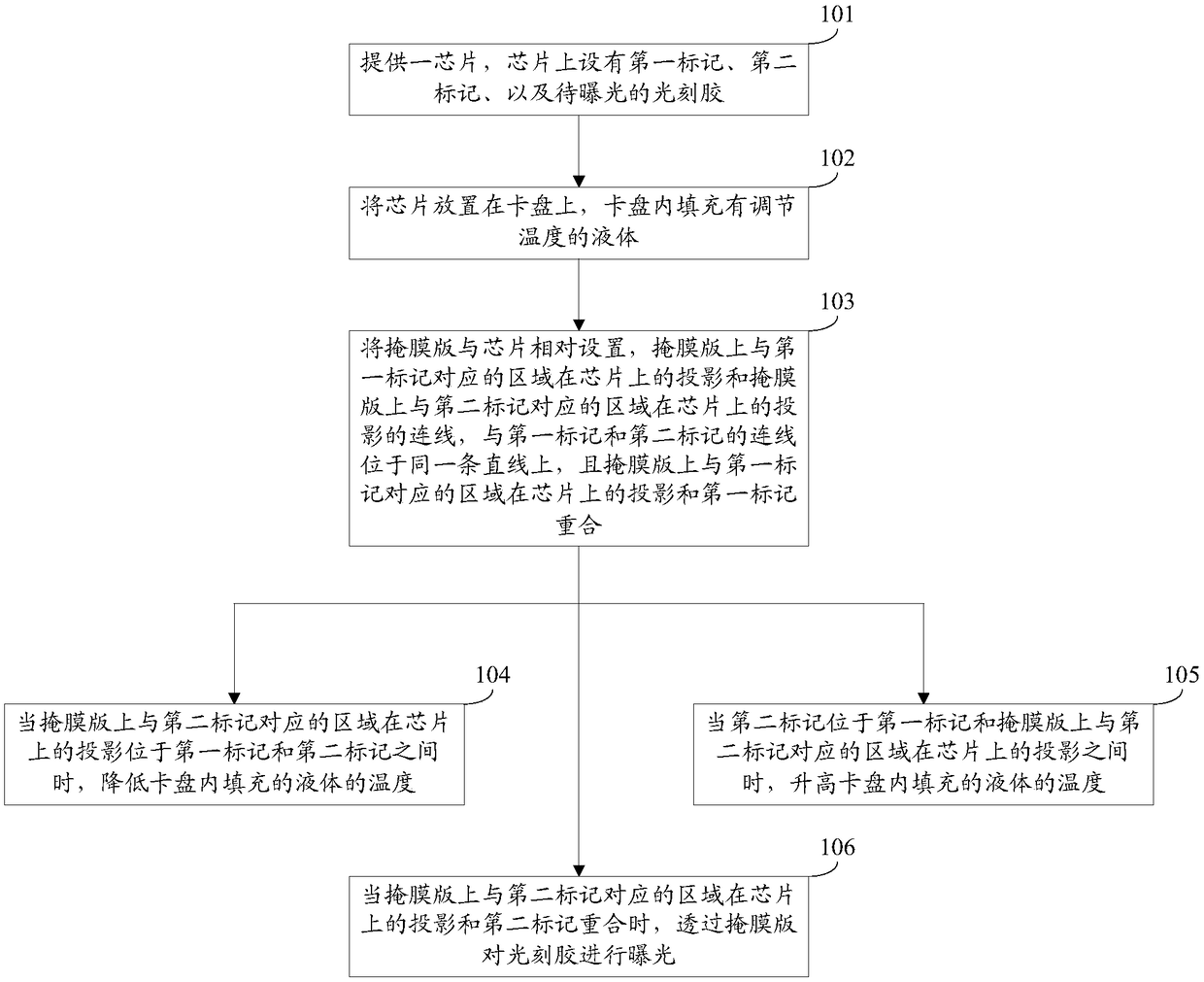
[0036] An embodiment of the present invention provides an exposure method. figure 1 It is a flow chart of an exposure method provided by an embodiment of the present invention. see figure 1 , the exposure method consists of:

[0037] Step 101: providing a chip on which a first mark, a second mark, and a photoresist to be exposed are provided.

[0038] Optionally, the connection line of the first mark and the second mark can be located on the center line of the chip, and the distance between the first mark and the second mark and the center of the chip can be equal, so that the first mark and the second mark can be used to connect The chip and the mask can be substantially aligned.

[0039] figure 2 A schematic structural diagram ...


PUM


Abstract

The invention discloses an exposure method, belonging to the field of semiconductor technology. Includes providing a chip with a first mark, a second mark and a photoresist to be exposed; Placing thechip on the chuck, and filling the chuck with a temperature regulating liquid; A mask plate is arrange opposite to that chip, and the projection of an area on the mask plate corresponding to the firstmark on the chip coincide with the first mark; Reducing the temperature of the liquid filled in the chuck when the projection of the area on the mask corresponding to the second mark on the chip is located between the first mark and the second mark; Raising the temperature of the liquid filled in the chuck when the second mark is located between the first mark and the projection on the chip of anarea on the mask corresponding to the second mark; When the projection of the area on the mask corresponding to the second mark on the chip coincides with the second mark, the photoresist is exposedthrough the mask. The invention can improve the misalignment of graphics.

Description

technical field [0001] The invention relates to the technical field of semiconductors, in particular to an exposure method. Background technique [0002] Light Emitting Diode (English: Light Emitting Diode, referred to as: LED) is a semiconductor electronic component that converts electrical energy into light energy. LED appeared in 1962. In the early days, it could only emit low-intensity red light, and later developed LEDs that emitted other monochromatic lights. Since gallium nitride (GaN)-based LEDs were successfully developed by Japanese scientists in the 1990s, the technology of LEDs has been continuously improved, the brightness of LEDs has been continuously improved, and the application fields of LEDs have become wider and wider. LED has the advantages of low voltage, low power consumption, small size, light weight, long life, high reliability, etc., and is rapidly and widely used in traffic lights, automotive interior and exterior lights, urban landscape lighting, ...

Claims


Application Information

Patent Timeline
IPC IPC(8): G03F7/20G03F9/00H01L21/68H01L33/00
CPCG03F7/70733G03F7/70775G03F9/7084H01L21/682H01L33/005
Inventor 兰叶顾小云
Owner HC SEMITEK ZHEJIANG CO LTD
Features
  • R&D
  • Intellectual Property
  • Life Sciences
  • Materials
  • Tech Scout
  • Unparalleled Data Quality
  • Higher Quality Content
  • 60% Fewer Hallucinations
Learn More