A unidirectional carrier photoelectric mixer and electromagnetic wave phased array antenna receiving front end

A single-line carrier and mixer technology, applied in circuits, electrical components, semiconductor devices, etc., can solve the problems of large photoelectric mixing loss, low device speed, low frequency, etc., and achieve the effect of large bandwidth loss

Active Publication Date: 2020-04-21
SOUTHEAST UNIV
View PDF7 Cites 0 Cited by
  • Summary
  • Abstract
  • Description
  • Claims
  • Application Information

AI Technical Summary

Problems solved by technology

For a single row carrier photodiode with a traditional structure, the linearity of the device is very high, but the nonlinearity is very weak, so the loss of photoelectric mixing is very large
In addition, the existing phototransistor can also realize photoelectric mixing, but the electrons and holes recombine in the base area. Due to the low mobility of the holes, the speed of the device is not high, and the recombination of electrons and holes will lead to low frequency generation-composite noise

Method used


Image

  • A unidirectional carrier photoelectric mixer and electromagnetic wave phased array antenna receiving front end
  • A unidirectional carrier photoelectric mixer and electromagnetic wave phased array antenna receiving front end
  • A unidirectional carrier photoelectric mixer and electromagnetic wave phased array antenna receiving front end

Examples


Embodiment 1

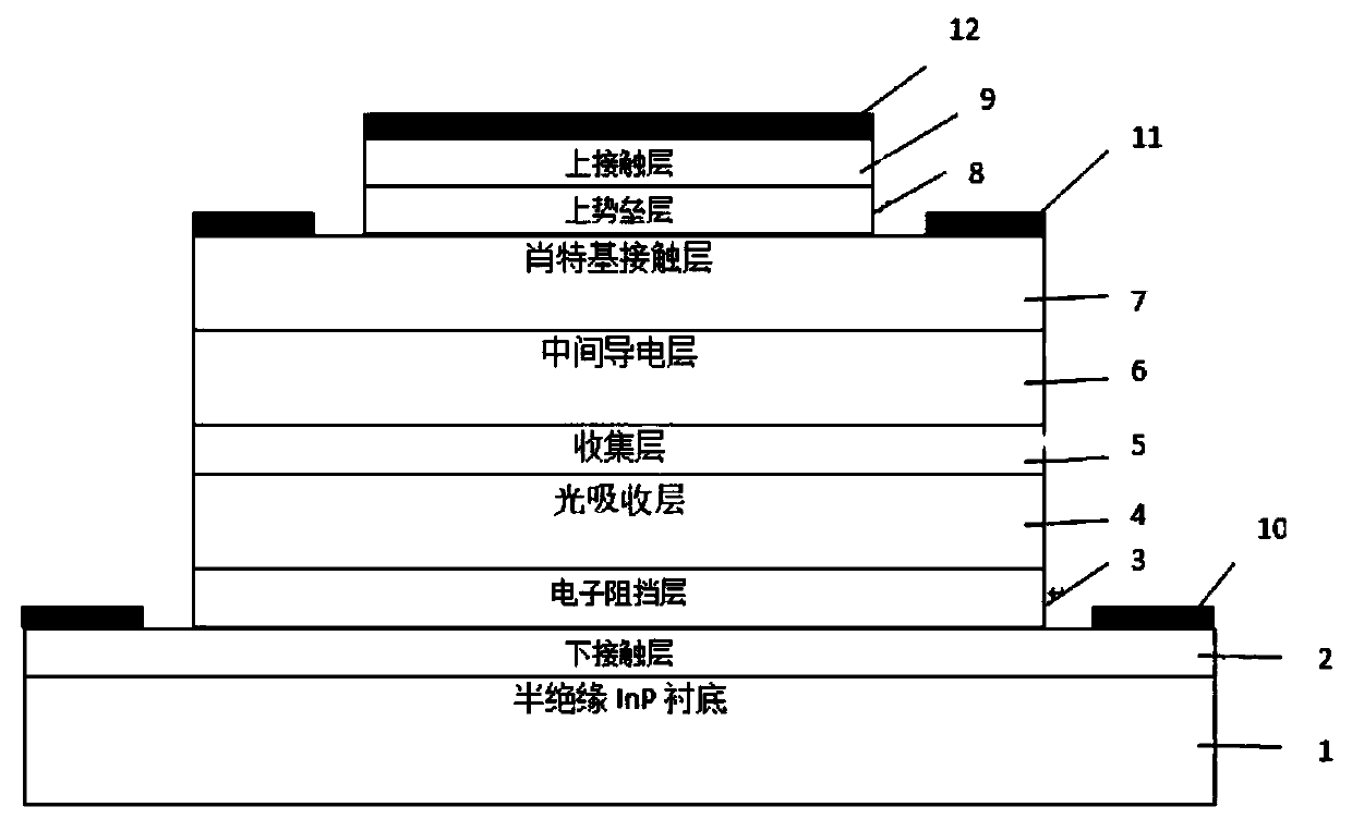
[0091] figure 1 It is a schematic diagram of the epitaxial layer structure of the single row carrier photoelectric mixer in the specific embodiment 1 of the present invention. combine figure 1 As shown, in this embodiment, the single row carrier optoelectronic mixer includes:

[0092] The semi-insulating substrate 1 is an InP semi-insulating substrate;

[0093] The P-type heavily doped lower contact layer 2 located on the upper surface of the semi-insulating substrate is a P-type heavily doped InGaAs layer;

[0094] The P-type heavily doped electron blocking layer 3 located on the upper surface of the P-type heavily doped lower contact layer is a P-type heavily doped InP layer;

[0095] The lower electrode metal layer 10 located on the upper surface of the P-type heavily doped lower contact layer and on both sides of the P-type heavily doped electron blocking layer;

[0096] The light absorbing layer 4 located on the upper surface of the P-type heavily doped electron block...

Embodiment 2

[0115] combine Figure 6 As shown, the single row carrier opto-electric mixer consists of:

[0116] The semi-insulating substrate 1 is an InP semi-insulating substrate;

[0117] The P-type heavily doped lower contact layer 2 located on the upper surface of the semi-insulating substrate is P-type heavily doped InGaAs;

[0118] The P-type heavily doped electron blocking layer 3 located on the upper surface of the P-type heavily doped lower contact layer is a P-type heavily doped InP layer;

[0119] The lower electrode metal layer 10 located on the upper surface of the P-type heavily doped lower contact layer and on both sides of the P-type heavily doped electron blocking layer;

[0120] The light absorbing layer 4 located on the upper surface of the P-type heavily doped electron blocking layer is a P-type gradiently doped InGaAs layer;

[0121] The collection layer 5 located on the upper surface of the light absorption layer is a low-doped N-type InP layer;

[0122] The N-ty...

Embodiment 3

[0144] like Figure 9 As shown in , the unit in the dotted box is a specific implementation method of delay / phase shift network and synthesis. Output signal e after photoelectric mixing m,i (i=0,1,2,...N) first pass through the low noise amplifier LNA i (i=0,1,2,...N) to amplify, and then pass through the electric phase shifter / delay device D i (i=0,1,2,...N) Delay different channels so that each channel outputs an electrical signal e after frequency conversion mp,i The phases of (i=0,1,2,...N) are all at time t, and the electrical signals of different channels are superimposed in the same phase in the power combiner, and then the signals are sent to the signal processing unit for further signal processing.


PUM

PropertyMeasurementUnit
thicknessaaaaaaaaaa
thicknessaaaaaaaaaa
thicknessaaaaaaaaaa

Abstract

The invention discloses a single-line carrier photoelectric mixer and a phased array antenna receiving front end, A substrate, a P-type heavily dope lower contact layer, a P-type heavily doped electron blocking layer, a light absorption layer, a collecting layer, an N-type heavily doped intermediate conductive layer, a Schottky contact layer, an N-type doped upper barrier layer and an N-type heavily doped upper contact layer are sequentially superposed on that single-row carrier photoelectric mixer from bottom to top. Further, the light absorbing layer is gradient doped. A moderately doped InPcliff layer is also arranged between the collecting layer and the light absorbing layer. By designing the material and the device structure, the invention has the advantages of high speed, large bandwidth, low photoelectric mixing frequency conversion loss, large bandwidth and low noise compared with the traditional single-row carrier photodiode, and is larger than that of the phototransistor.

Description

technical field [0001] The invention relates to the technical field of semiconductor photoelectric devices, in particular to a unidirectional carrier photoelectric mixer and an electromagnetic wave phased array antenna receiving front end. Background technique [0002] A photodetector is a device that converts optical signals into electrical signals. When the photon energy of the incident optical signal is greater than the band gap of the light-absorbing layer material, photogenerated carriers will be generated in the photodetector. At this time, if an AC signal is superimposed on the bias voltage of the photodetector to modulate the photogenerated carriers, the frequency mixing of the input optical signal and the AC signal superimposed on the bias voltage of the photodetector can be realized. The photoelectric mixing in a large number of literatures is to use the nonlinear relationship between the output response of the photodetector and the bias voltage and the incident li...

Claims


Application Information

Patent Timeline
Patent Type & Authority Patents(China)
IPC IPC(8): H01L31/101H01L31/0304H04B1/18
CPCH01L31/03042H01L31/03046H01L31/101H04B1/18
Inventor 杨春贾少鹏宋振杰
Owner SOUTHEAST UNIV
Why Eureka
Try Eureka