Organic light emitting device

A technology of organic light-emitting devices and light-emitting layers, which is applied in the manufacture of electric solid-state devices, semiconductor devices, semiconductor/solid-state devices, etc., and can solve the problems of low luminous efficiency of light-emitting devices, low recombination efficiency of electrons and holes, and unbalanced carrier injection and other issues to achieve the effect of improving luminous efficiency and service life, avoiding heat accumulation, and avoiding imbalance

Active Publication Date: 2019-01-25
CHANGCHUN HYPERIONS TECH CO LTD
View PDF5 Cites 1 Cited by
  • Summary
  • Abstract
  • Description
  • Claims
  • Application Information

AI Technical Summary

Problems solved by technology

[0004] However, traditional OLED display devices often have problems with luminous efficiency and service life. The main reasons are as follows: on the one hand, it depends on the luminous performance of the organic light-emitting materials used, and the matching degree between the composite materials of each layer; on the other hand, it depends on Exciton utilization, due

Method used


Image

  • Organic light emitting device
  • Organic light emitting device
  • Organic light emitting device

Examples


Embodiment 1

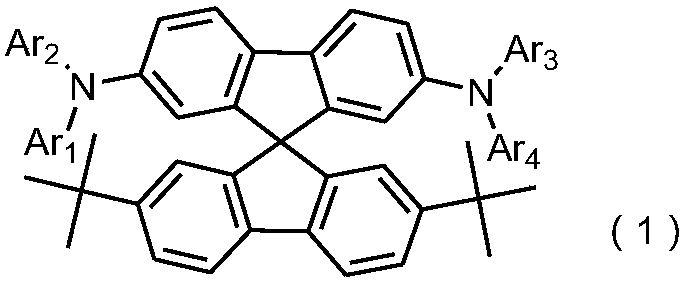
[0096] Embodiment 1: the synthesis of compound 1

[0097]

[0098] Synthesis of compound 1

[0099] To compound a (107.3 g , 183 mmol) and diphenylamine (62.0 g, 367 mmol) in degassed toluene (1 L), and the mixture was heated at reflux for 2 hours. The reaction mixture was cooled to room temperature, diluted with toluene and filtered through celite. The filtrate was diluted with water and extracted with toluene, and the combined organic phases were evaporated under vacuum. The residue was filtered through silica gel and recrystallized. Compound 1 (111.5 g, yield 80%) was obtained.

[0100] Mass Spectrum m / z: 762.43 (calculated: 762.40). Theoretical element content (%)C 57 h 50 N 2 : C, 89.72; H, 6.60; N, 3.67 The measured element content (%): C, 89.74; H, 6.61; N, 3.65. The above results confirmed that the obtained product was the target product.

Embodiment 2

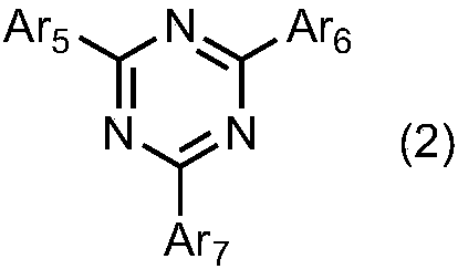
[0101] Embodiment 2: the synthesis of compound 8

[0102]

[0103] Preparation of Intermediate C

[0104] To compound a (107.3 g , 183 mmol) and Intermediate A (57.2 g, 183 mmol) in degassed toluene (1 L), and the mixture was heated at reflux for 2 h. The reaction mixture was cooled to room temperature, diluted with toluene and filtered through celite. The filtrate was diluted with water and extracted with toluene, and the combined organic phases were evaporated under vacuum. The residue was filtered through silica gel and recrystallized. Intermediate C (115.0 g, 80% yield) was obtained.

[0105] Mass Spectrum m / z: 786.90 (calculated: 786.92). Theoretical element content (%)C 53 h 56 BrN: C, 80.89; H, 7.17; Br, 10.15; N, 1.78 Measured element content (%): C, 80.88; H, 7.17; Br, 10.17; N, 1.78. The above results confirmed that the obtained product was the target product.

[0106] Preparation of compound 8

[0107] To intermediate C (143.8 g, 183 mmol) and intermed...

Embodiment 3

[0109] Embodiment 3: the synthesis of compound 13

[0110]

[0111] The intermediate A in Example 2 was replaced with an equimolar intermediate A-2, and the other steps were the same as in Example 2 to obtain the target compound 13. Mass Spectrum m / z: 1031.26 (calculated: 1031.37). Theoretical element content (%)C 78 h 66 N 2 : C, 90.83; H, 6.45; N, 2.72 Measured element content (%): C, 90.86; H, 6.44; N, 2.71. The above results confirmed that the obtained product was the target product.


PUM

PropertyMeasurementUnit
Thicknessaaaaaaaaaa
Thicknessaaaaaaaaaa

Abstract

The invention provides an organic light emitting device, which relates to the technical field of organic photoelectricity. An organic light emitting device is provided in which a hole transport layercomprises a first compound represented by the formula (1) and an electron transport layer comprises a second compound represented by the formula (2). On the one hand, fluorene groups are three-dimensional structures, which make the compounds difficult to crystallize; Spirobifluorene group is substituted by tert-butyl group, which increases the solubility of the compound, and this structure has a ductile conjugated system, which has better carrier transport properties. On the one hand, triazine groups are combined with fluorene groups, and the continuous Phi conjugated system makes the structure have high electron mobility. By combining the first compound and the second compound, the transmission rate of electrons and holes is balanced, the generation rate and utilization rate of excitons in the luminescent layer are improved, the on-voltage of the device is reduced, and the luminescent efficiency and the service life of the device are improved.

Description

technical field [0001] The invention relates to the field of organic photoelectric technology, in particular to an organic light emitting device. Background technique [0002] In recent years, Organic Light Emitting Diode (OLED: Organic Light Emitting Diode) as a new and promising display technology has gradually entered people's field of vision. Compared with traditional display technologies, it has significant advantages in voltage characteristics, luminous brightness, luminous efficiency, device weight, response speed, and viewing angle, and has broad market prospects due to its low-cost potential. [0003] Typically, OLEDs have a layered or laminated structure. For example, a typical OLED has an anode / organic light-emitting layer / cathode multilayer structure. OLEDs can also have various other structures such as anode / hole injection layer / hole transport layer / light emitting layer / electron transport layer / electron injection layer / cathode multilayer structure or anode / hol...

Claims


Application Information

Patent Timeline
IPC IPC(8): H01L51/50H01L51/54
CPCH10K85/00H10K50/00H10K50/15H10K50/16
Inventor 刘喜庆蔡辉
Owner CHANGCHUN HYPERIONS TECH CO LTD
Why Eureka
Try Eureka