AI technical title is built by Patsnap AI team. It summarizes the technical point description of the patent document.
A technology of organic light-emitting devices and light-emitting layers, which is applied in the manufacture of semiconductor devices, electric solid-state devices, and semiconductor/solid-state devices. rate, to avoid unbalanced effects
Active Publication Date: 2020-10-09
CHANGCHUN HYPERIONS TECH CO LTD
View PDF4 Cites 0 Cited by
Summary
Abstract
Description
Claims
Application Information
AI Technical Summary
This helps you quickly interpret patents by identifying the three key elements:
Problems solved by technology
Method used
Benefits of technology
Problems solved by technology
Since the transport velocity of electrons is lower than that of holes, the carriers in the light-emitting layer are not matched, resulting in a significant decline in device performance, which affects the reduction in device efficiency and the shortening of life.
Method used
Image
Click on the blue label to locate the original text in one second.
Reading with bidirectional positioning of images and text.
[0101] The organic light-emitting device of the present invention can be widely used in the fields of panel display, lighting source, flexible OLED, electronic paper, organic photoreceptor or organic thin film transistor, signboard, signal lamp and the like.
Embodiment 1
[0104] [Example 1] Synthesis of Compound 1-3
[0105]
[0106] Step1: Add compound 1-3-e (12.71g, 37.6mmol) to the reactor and dissolve in tetrahydrofuran (140mL), add dropwise hexanesolvent and 2.5M n-butyllithium (18mL, 45.1mmol) at -78°C ), stirred for 1 hour. After slowly adding trimethyl borate (13 mL, 56.4 mmol) dropwise, stirred for 2 h. Then 2M hydrochloric acid was added dropwise to neutralize, and the product was extracted with ethyl acetate and water. Recrystallization from dichloromethane and hexane gave compound 1-3-A (4.73 g, 47%).
[0107] Step2: Add compound 1-3-A (28.81g, 100mmol), compound 1-3-g (12.30g, 100mmol), tetrakistriphenylphosphine palladium (1.15g, 1mmol) and sodiumcarbonate (41.4g) in the reactor , 300 mmol), the weighed reactant was dissolved in a solvent of toluene (1 L) / EtOH (200 mL) / distilled water (200 mL), and heated at 90° C. for 2 hours. The reaction mixture was cooled to room temperature, diluted with toluene and filtered through ...
Embodiment 2
[0111] [Example 2] Synthesis of Compound 1-5
[0112] Compound 1-3-g in compound 1-3 in Example 1 was replaced by equimolar compound 1-5-g, and compound 1-5 (36.57 g, 58%) was obtained according to the synthesis method of compound 1-3.
[0113]
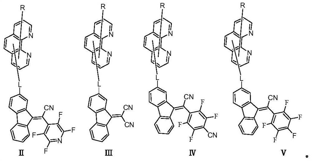
[0114] Mass Spectrum m / z: 630.16 (calculated: 630.15). Theoretical element content (%)C 40 h 18 f 4 N 4 : C, 76.19; H, 2.88; F, 12.05; N, 8.88 The measured element content (%): C, 76.19; H, 2.88; F, 12.06; N, 8.87. The above results confirmed that the obtained product was the target product.
PUM
Abstract
The invention provides an organic light-emitting device and relates to the technical field of organic photoelectricity. The device of the present invention is a double-layer electron transport device structure, which comprises o-phenanthroline compounds as the first electrontransport layer and heterocyclic compounds as the second electrontransport layer. The first electron transport layer and the second electron transport layer are combined to increase the electron transport rate, increase the generation rate and utilization rate of excitons in the light-emitting layer, avoid the imbalance of carriers in the light-emitting layer, and avoid the electron transport layer The deterioration of device life caused by heat accumulation at the interface with the light-emitting layer significantly improves the luminous efficiency of the organic light-emitting device and significantly reduces the driving voltage. It is an organic light-emitting device with excellent performance and can be widely used in the display field.
Description
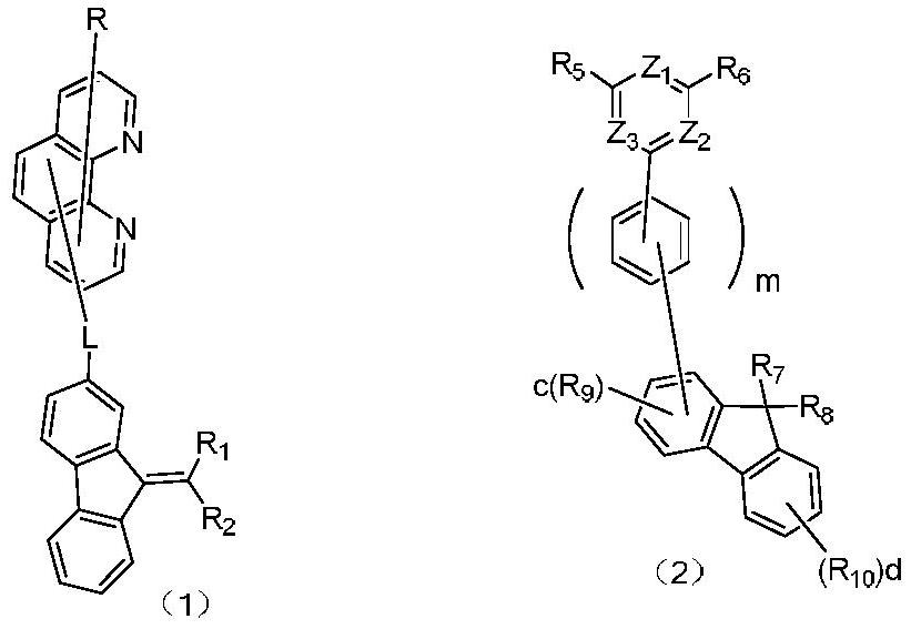
technical field [0001] The invention relates to the technical field of organic electroluminescence, in particular to an organic light emitting device. Background technique [0002] In 1987, Tang et al. of Kodak Company invented a sandwich-type organic double-layer thin-film light-emitting device. This breakthrough made people see the huge potential of OLED technology to be practical and commercialized, and set off a research boom of organic light-emitting diodes. Over the past 30 years, OLED technology has achieved rapid development, and has moved from laboratory research to industrial production. [0003] At present, the development of OLED materials has reached a relatively mature stage, and material companies at home and abroad provide hundreds of innovative materials for selection. Organic charge transport materials are a class of organic semiconductor materials that can achieve controllable directional and ordered migration of carriers under the action of an electric f...
Claims
Application Information
Patent Timeline
Application Date:The date an application was filed.
Publication Date:The date a patent or application was officially published.
First Publication Date:The earliest publication date of a patent with the same application number.
Issue Date:Publication date of the patent grant document.
PCT Entry Date:The Entry date of PCT National Phase.
Estimated Expiry Date:The statutory expiry date of a patent right according to the Patent Law, and it is the longest term of protection that the patent right can achieve without the termination of the patent right due to other reasons(Term extension factor has been taken into account ).
Invalid Date:Actual expiry date is based on effective date or publication date of legal transaction data of invalid patent.

