Manufacturing method of double-sided multi-step cavity LTCC substrate

A manufacturing method and multi-step technology, applied in semiconductor/solid-state device manufacturing, electrical solid-state devices, semiconductor devices, etc., can solve problems such as short interconnection paths, parasitic interference of radio frequency signals, and affecting circuit performance, so as to improve electrical performance, Effects of improving performance and ensuring lamination accuracy

Active Publication Date: 2019-01-29
XIAN MICROELECTRONICS TECH INST
View PDF5 Cites 4 Cited by
  • Summary
  • Abstract
  • Description
  • Claims
  • Application Information

AI Technical Summary

Problems solved by technology

For highly integrated SiP products and LTCC RF / microwave products, the interconnection path between chips and components is required to be as short as possible. Conventional single-sided structures can only assemble chips on one side of the substrate, or inside the cavity on one side, resulting in The size cannot be reduced, the interconnection leads cannot be shortened, and the radio frequency signal will also generate parasitic interference, which will affect the performance of the circuit

Method used


Image

  • Manufacturing method of double-sided multi-step cavity LTCC substrate
  • Manufacturing method of double-sided multi-step cavity LTCC substrate
  • Manufacturing method of double-sided multi-step cavity LTCC substrate

Examples


Embodiment Construction

[0037] The present invention is described in further detail below in conjunction with accompanying drawing:

[0038] The specific manufacturing method is as follows:

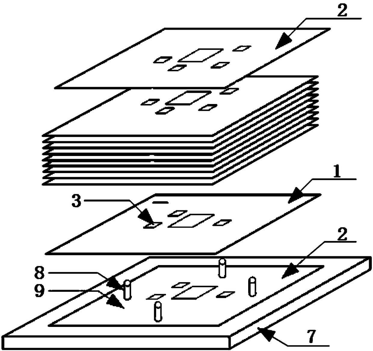
[0039] The first step: if figure 1 As shown, the green ceramic sheet 1 is pre-dried, punched and opened, filled and printed with conductors, and dried with metal conductors according to the traditional process.

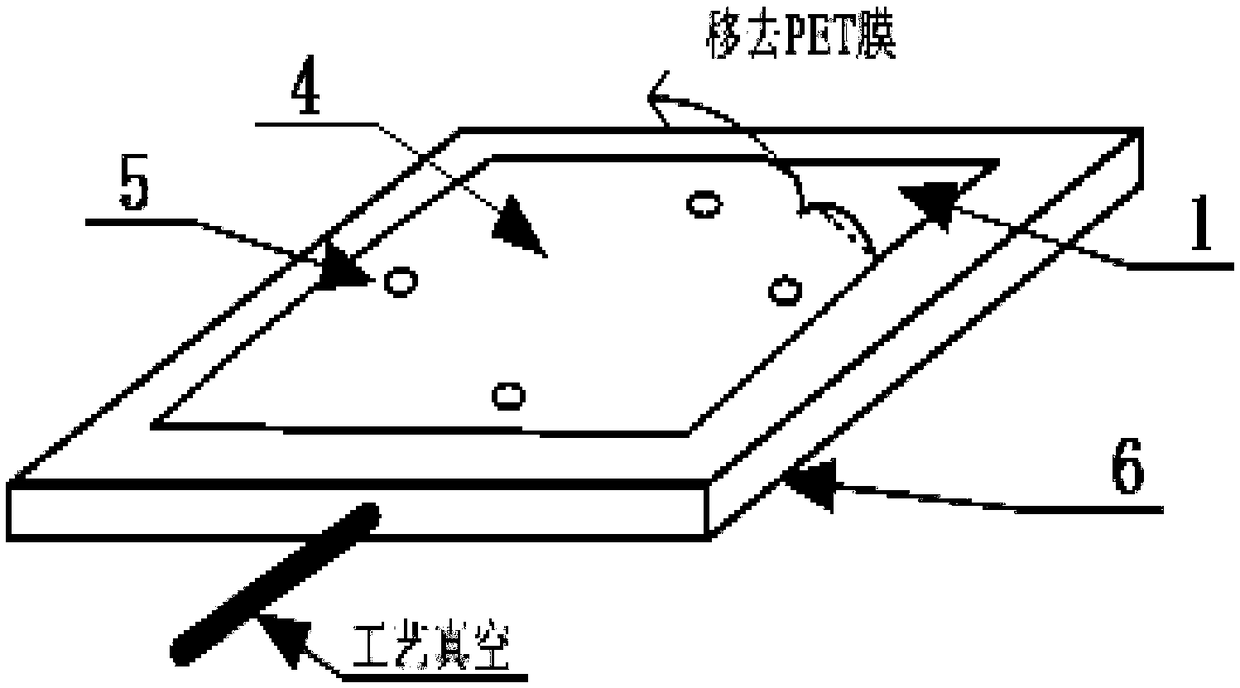
[0040] Part 2: Release treatment of green ceramic sheet 1;

[0041] Such as figure 2 As shown, the green ceramic sheet 1 is adsorbed on the suction cup 6 by process vacuum during demoulding, and then the PET film 4 of the green ceramic sheet 1 is removed, and then the adsorption is cancelled, and the green ceramic sheet 1 is removed.

[0042] When the suction cup 6 absorbs the green ceramic sheet 1, the position of the cavity 3 of the green ceramic sheet 1 should be staggered to prevent the suction force from decreasing.

[0043] The third step: 1 stack of green ceramic sheets is used as the substr...


PUM

PropertyMeasurementUnit
thicknessaaaaaaaaaa
thicknessaaaaaaaaaa

Abstract

The invention discloses a manufacturing method of a double-sided multi-step cavity LTCC substrate, which comprises the steps of 1, carrying out pre-drying, punching, cavity setting, hole filling, conductor printing and metal conductor drying on green ceramic chips; 2, carrying out film removal processing on the green ceramic chips; 3, laminating, that is, laminating the green ceramic chips to serve as a substrate, wherein the upper and lower surface cavities of the substrate are sequentially reduced in area from the surface to the center and area isolated by the green ceramic chips without a cavity, metal sheets are placed on the top and bottom of the substrate and form an integral whole so as to serve as a green ceramic blank; 4, carrying out vacuum packaging on the green ceramic blank; 5, carrying out isostatic pressing lamination on the vacuum packaged green ceramic blank; 6, taking out the substrate after completing isostatic pressing lamination, carrying out thermal cutting on thesubstrate to cut a required pattern and size, removing redundant corners, and cutting out a filling block; and 7, placing the filling block in the innermost layer cavity at the bottom of the substrate, and placing the bottom of the substrate on a bearing plate in a sintering furnace for low-temperature sintering.

Description

technical field [0001] The invention belongs to the technical field of semiconductor hybrid integrated circuits, and relates to a method for manufacturing an LTCC substrate with a double-sided multi-step cavity. Background technique [0002] Usually, there are no cavities in the LTCC substrate, or the cavities are arranged on one side of the substrate, and the other side does not contain cavities. For highly integrated SiP products and LTCC RF / microwave products, the interconnection path between chips and components is required to be as short as possible. Conventional single-sided structures can only assemble chips on one side of the substrate, or inside the cavity on one side, resulting in The size cannot be reduced, the interconnection leads cannot be shortened, and the radio frequency signal can also generate parasitic interference, which in turn affects the performance of the circuit. Contents of the invention [0003] The purpose of the present invention is to overco...

Claims


Application Information

Patent Timeline
Patent Type & Authority Applications(China)
IPC IPC(8): H01L23/15H01L21/48
CPCH01L21/4807H01L21/481H01L23/15
Inventor 肖刚刘发李建国陈宁
Owner XIAN MICROELECTRONICS TECH INST
Why Eureka
Try Eureka