

Thin 3D fan-out packaging structure and wafer-level packaging method
A technology of wafer-level packaging and packaging structure, which is applied in the manufacture of electrical components, electrical solid-state devices, semiconductor/solid-state devices, etc. It can solve the problems that the height of stacked packaging cannot be further reduced, the quality of lining preparation is difficult to ensure, and the yield rate is difficult to improve. , to achieve the effect of solving deposition quality problems, aligning accurately, and reducing stack thickness
- Summary
- Abstract
- Description
- Claims
- Application Information
AI Technical Summary
Problems solved by technology
Method used
Image

Examples
Embodiment Construction
[0036] In order to understand the technical content of the present invention more clearly, the following examples are given in detail, the purpose of which is only to better understand the content of the present invention but not to limit the protection scope of the present invention. The components in the structures in the drawings of the embodiments are not scaled according to the normal scale, so they do not represent the actual relative sizes of the structures in the embodiments.
[0037] A thin 3D fan-out wafer level packaging method, comprising the steps of:
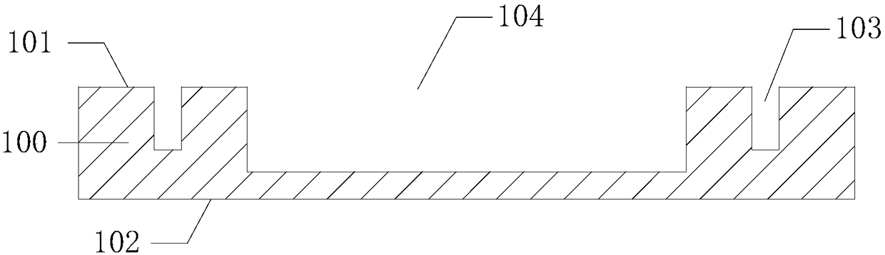
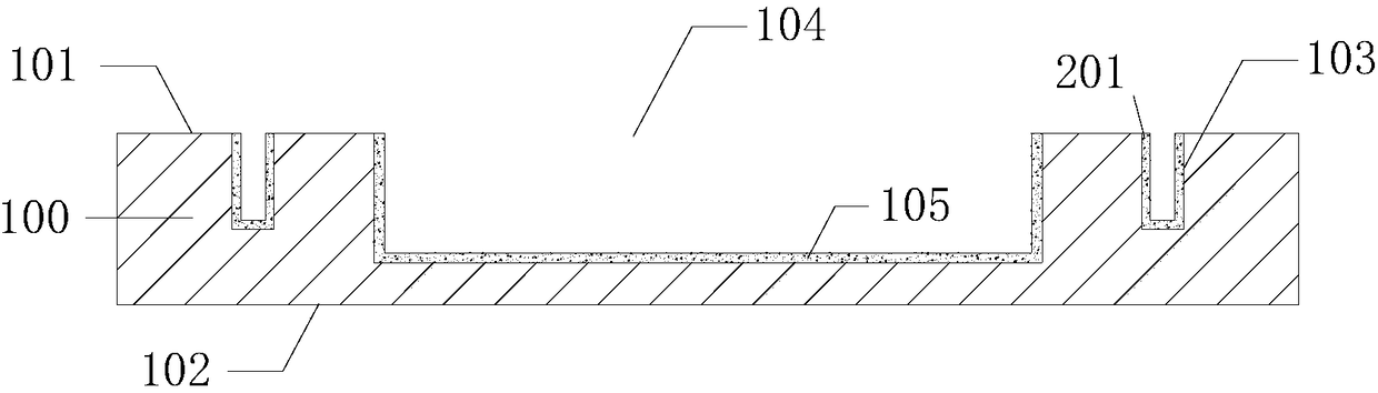
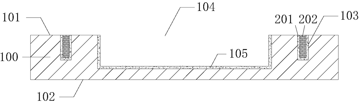
[0038] A. see Figure 1a , providing a carrier 100, the carrier has a first surface 101 and a second surface 102 opposite thereto, at least one groove 104 extending toward the second surface 102 is formed on the first surface 101 of the carrier, and A plurality of blind holes 103 whose depth is not greater than the groove.
[0039] The carrier generally uses silicon wafers, and grooves and blind holes are formed b...
PUM
 Abstract
Description
Claims
Application Information