2D semiconductor heterojunction based AND/OR logic gate circuit and realization and preparation methods thereof
A technology of two-dimensional semiconductors and logic gate circuits, applied in the field of nanoelectronics
- Summary
- Abstract
- Description
- Claims
- Application Information
AI Technical Summary
Problems solved by technology
Method used
Image

Examples
Embodiment 1
[0048] Example 1. Preparation of devices for forming AND / OR logic gates based on two-dimensional semiconductor heterojunctions
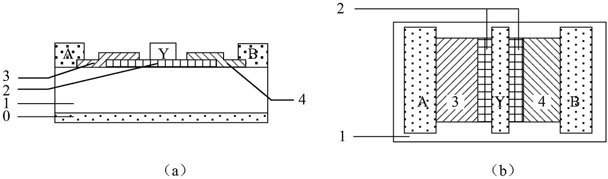
[0049] Such as image 3 As shown, the device part of the AND / OR logic gate circuit based on the two-dimensional semiconductor heterojunction in this embodiment includes a gate electrode 0, an insulating substrate 1, and a first two-dimensional semiconductor material 2 on the insulating substrate 1. The material There is a second two-dimensional semiconductor material 3 and a third two-dimensional semiconductor material 4 above to form a vertical stack, the first metal electrode A is located above the second two-dimensional semiconductor material 3, and the second metal electrode B is located on the third two-dimensional semiconductor material 4, the third metal electrode Y is located above the first two-dimensional semiconductor material 2.
[0050] The method for preparing the device part of the above-mentioned two-dimensional semiconductor heteroj...
Embodiment 2
[0058] Embodiment 2. Realization of an AND / OR logic gate circuit based on a two-dimensional semiconductor heterojunction
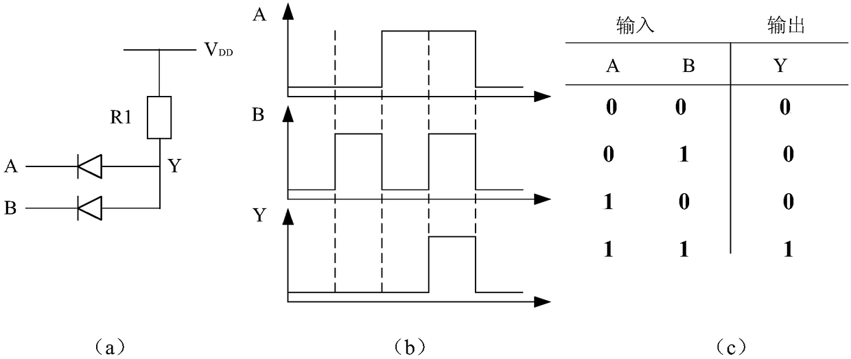
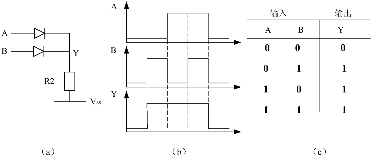
[0059] The third metal electrode of the two-dimensional semiconductor heterojunction device prepared in Example 1 is externally connected with a fixed resistor (R1 or R2) to form an AND / OR logic gate circuit. When realizing the AND logic function, one end of the external fixed resistor R1 is connected to the common electrode of the device—the third metal electrode Y, and the other end is connected to the power supply voltage V DD ,Such as figure 1 As shown; when implementing the OR logic function, one end of the external fixed resistor R2 is connected to the third metal electrode Y of the device, and the other end is grounded V SS ,Such as figure 2 shown.
[0060] For AND logic, see figure 1 , image 3 with Figure 5 In (a), the realization process is as follows: when the grid voltage V G When it is a negative value, the first two-dimensional semic...
Embodiment 3
[0062] Embodiment 3. Implementation of a dual-function AND / OR logic gate circuit based on a two-dimensional semiconductor heterojunction
[0063] The third metal electrode Y of the two-dimensional semiconductor heterojunction device prepared in Example 1 is externally connected with a PMOS transistor M1, an NMOS transistor M2, and two fixed resistors R1 and R2 to form a dual-function AND / OR logic gate circuit. The PMOS transistor M1 and the NMOS transistor M2 share a gate electrode with the two-dimensional semiconductor heterojunction device. The drain terminal of the PMOS transistor M1 is connected to the common electrode of the device—the third metal electrode Y, the source terminal is connected to a fixed resistor R1, and the other end of R1 is connected to the power supply voltage V DD . The drain terminal of the NMOS transistor M2 is connected to the common electrode of the device—the third metal electrode Y, the source terminal is connected to the fixed resistor R2, and...
PUM
 Abstract
Description
Claims
Application Information
PatSnap Eureka turns technology decisions into work you can execute. Powered by our Innovation Knowledge Graph, it runs expert workflows across engineering, life sciences, materials and intellectual property. Get your review-ready output in minutes.


