Method for preparing zno/cu2o heterojunction material and zno/cu2o three-dimensional structure heterojunction solar cell

A three-dimensional structure, heterojunction technology, applied in sustainable manufacturing/processing, circuits, electrical components, etc., can solve problems such as insufficient carrier transport and separation, short collection length of photogenerated carriers, limiting cell efficiency, etc. , to achieve the effect of excellent overall performance, high photoelectric conversion efficiency and abundant resources

Inactive Publication Date: 2011-12-07
UNIV OF JINAN
View PDF1 Cites 32 Cited by
  • Summary
  • Abstract
  • Description
  • Claims
  • Application Information

AI Technical Summary

Problems solved by technology

Cu 2 The O resistance is higher and the photogenerated carrier collection length is shorter, and the Cu at the top of the rod 2 Carriers generated by O absorption of photons cannot be fully transported and separated
In addition, Cu 2 The filling of O between the nanorods is not filled from bottom to top along the direction of the nanorods, the density is less, and the interface defects are more
These problems all limit the battery efficiency

Method used


Image

  • Method for preparing zno/cu2o heterojunction material and zno/cu2o three-dimensional structure heterojunction solar cell
  • Method for preparing zno/cu2o heterojunction material and zno/cu2o three-dimensional structure heterojunction solar cell
  • Method for preparing zno/cu2o heterojunction material and zno/cu2o three-dimensional structure heterojunction solar cell

Examples


Embodiment 1

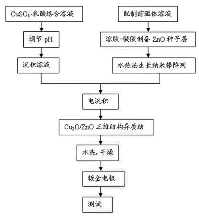
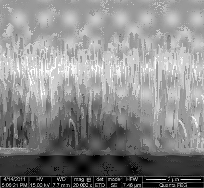
[0055] (1) The ZnO nanorod array was grown by hydrothermal method on the ITO conductive substrate, the seed layer thickness was 150nm, the rod length was 4μm, the rod spacing was 150nm, and the rod diameter was 150.

[0056] (2) Preparation of p-type Cu 2 O semiconductor precursor solution to CuSO 4 solution as a precursor solution, adding lactic acid as a stabilizer, where CuSO 4 The concentration of lactic acid is 0.2mol / L, the concentration of lactic acid is 3mol / L, and the pH of the solution is adjusted to 10.5 with NaOH;

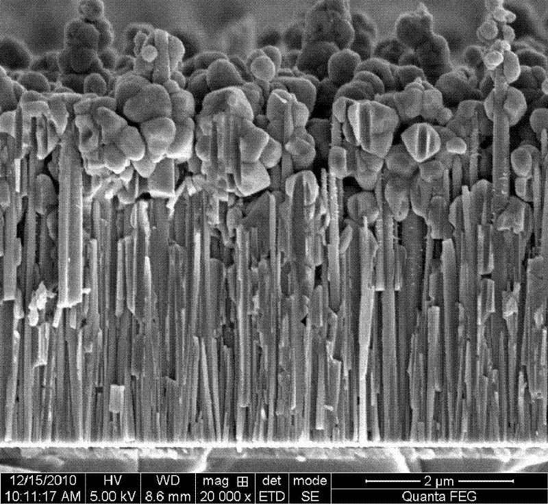
[0057] (3) Electrochemical conformal deposition of Cu on the surface of ZnO nanorods using the above precursor solution as the electrolyte 2 O seed layer, the conditions of the deposition process are: temperature 25°C, deposition potential -0.4V, deposition time 100s.

[0058] (4) Preparation of p-type Cu 2 O semiconductor deposition solution to CuSO 4 solution as a deposition solution, adding lactic acid as a stabilizer, where CuSO 4 The concentr...

Embodiment 2

[0062] (1) ZnO nanorod arrays were grown hydrothermally on the ITO conductive substrate, the seed layer thickness was 100nm, the rod length was 4μm, the rod spacing was 100nm, and the rod diameter was 50nm.

[0063] (2) Preparation of p-type Cu 2 O semiconductor precursor solution to CuSO 4 solution as a precursor solution, adding lactic acid as a stabilizer, where CuSO 4 The concentration of lactic acid is 0.2mol / L, the concentration of lactic acid is 3mol / L, and the pH of the solution is adjusted to 9.0 with NaOH;

[0064] (3) Electrochemical conformal deposition of Cu on the surface of ZnO nanorods using the above precursor solution as the electrolyte 2 O seed layer, the conditions of the deposition process are: temperature 15°C, deposition potential -0.5V, deposition time 100s.

[0065] (4) Preparation of p-type Cu 2 O semiconductor deposition solution to CuSO 4 solution as a deposition solution, adding lactic acid as a stabilizer, where CuSO 4 The concentration of l...

Embodiment 3

[0068] (1) The ZnO nanorod array was grown by hydrothermal method on the ITO conductive substrate, the seed layer thickness was 150nm, the rod length was 4μm, the rod spacing was 150nm, and the rod diameter was 150.

[0069] (2) Preparation of p-type Cu 2 O semiconductor precursor solution to CuSO 4 solution as a precursor solution, adding lactic acid as a stabilizer, where CuSO 4The concentration of lactic acid is 0.2mol / L, the concentration of lactic acid is 3mol / L, and the pH of the solution is adjusted to 9.0 with NaOH;

[0070] (3) Electrochemical conformal deposition of Cu on the surface of ZnO nanorods using the above precursor solution as the electrolyte 2 O seed layer, the conditions of the deposition process are: temperature 25°C, deposition potential -0.4V, deposition time 100s.

[0071] (4) Preparation of p-type Cu 2 O semiconductor deposition solution to CuSO 4 solution as a deposition solution, adding lactic acid as a stabilizer, where CuSO 4 The concentrat...


PUM

PropertyMeasurementUnit
thicknessaaaaaaaaaa

Abstract

The invention discloses a method for preparing a ZnO/Cu2O heterojunction material and a ZnO/Cu2O three-dimensional structure heterojunction solar cell. The preparation method of the heterojunction material includes growing an n-type ZnO nanorod array on a substrate by a liquid phase growth method Thin film, with alkaline copper salt solution as the electrolyte, deposited at a deposition potential of -0.4~-0.6V for 60-150s, and electrochemically deposited p-type Cu2O on the surface of ZnO nanorods to form a Cu2O seed layer; with alkaline copper The salt solution is the deposition solution. Under the deposition potential of -0.05 ~ -0.3V, the Cu2O is fully filled into the gaps of the nanorod array from bottom to top by the electrochemical deposition method again to form a ZnO/Cu2O three-dimensional structure heterojunction material. The filling depth and density of the Cu2O semiconductor thin film of the invention are increased, interface defects are reduced, and the efficiency of the prepared heterojunction battery is high.

Description

technical field [0001] The present invention relates to the preparation of ZnO / Cu 2 A method for a three-dimensional structure heterojunction material and a method for preparing a solar cell using the material, particularly involving filling p-type Cu in a (002)-oriented n-type ZnO semiconductor nanorod array using electrochemical deposition technology 2 Preparation of ZnO / Cu from O semiconductor 2 The invention relates to a three-dimensional structure heterojunction material and a battery device method, belonging to the technical fields of semiconductor devices and new energy sources. Background technique [0002] Cu 2 O is a semiconductor material that was discovered very early. It is a rare semiconductor material that can be excited by visible light. 2 O is non-toxic, abundant in reserves, low in preparation cost, high in theoretical utilization efficiency, and has important applications in electrode materials, catalysis, electronic devices, and gas sensors. Research ...

Claims


Application Information

Patent Timeline
Patent Type & Authority Applications(China)
IPC IPC(8): C25D7/12H01L31/18
CPCY02P70/50
Inventor 武卫兵李梅胡广达
Owner UNIV OF JINAN
Why Eureka
Try Eureka