A voltage doubling source circuit, a charge pump circuit and electronic equipment

A source circuit and capacitor technology, applied in the field of circuit design, can solve the problems of reducing the overall efficiency of the voltage doubler source circuit, reducing the efficiency of transistor transfer voltage, etc., to achieve the effect of avoiding body effect, improving efficiency, and improving overall efficiency

Active Publication Date: 2020-02-11
ZHUHAI CHUANGFEIXIN TECH CO LTD
View PDF7 Cites 0 Cited by
  • Summary
  • Abstract
  • Description
  • Claims
  • Application Information

AI Technical Summary

Problems solved by technology

The efficiency of the voltage doubling source circuit directly affects the overall power consumption of the chip using the voltage doubling source circuit. In the existing voltage doubling source circuit, due to the doping type Different, the substrate of the transistor can only be grounded, so that the source voltage of the transistor is greater than the substrate voltage, which leads to serious body effect, reduces the efficiency of these transistors to transfer voltage, and then reduces the overall efficiency of the voltage doubler source circuit

Method used


Image

  • A voltage doubling source circuit, a charge pump circuit and electronic equipment
  • A voltage doubling source circuit, a charge pump circuit and electronic equipment
  • A voltage doubling source circuit, a charge pump circuit and electronic equipment

Examples


Embodiment Construction

[0045] As mentioned in the background, in the existing voltage doubling source circuits, due to the difference in doping type between the transistors that transfer the voltage and the wafers used to prepare the voltage doubling source circuits, the problem of body effect is caused, which reduces the transfer of these transistors. The efficiency of the voltage reduces the overall efficiency of the voltage doubling source circuit.

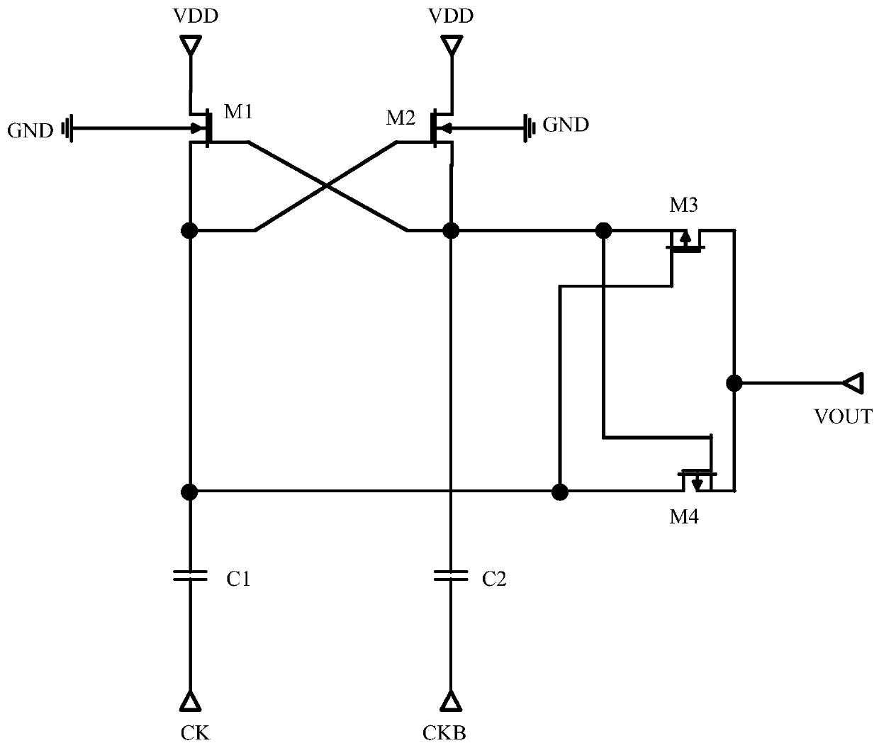
[0046] The specific principle is explained as follows, such as figure 1 as shown, figure 1 It is a schematic diagram of the circuit structure of the voltage doubling source circuit in the prior art, the voltage doubling source circuit is composed of a first transistor M1, a second transistor M2, a third transistor M3, a fourth transistor M4, a first capacitor C1 and a second capacitor C2 configuration, wherein the first transistor M1, the second transistor M2, the third transistor M3 and the fourth transistor M4 are cross-coupled and connected, and ...


PUM


Abstract

The application discloses a voltage doubling source circuit, a charge pump circuit and electronic equipment, wherein the voltage doubling source circuit uses a P-type transistor as a voltage transfer transistor, and the P-type transistor is based on an N well, and the N well can be Connect any potential higher than the ground, so the base of the P-type transistor can be directly connected to the source of the P-type transistor, avoiding the fact that the source voltage of the N-type transistor that functions as a voltage transfer is higher than that of the existing CMOS type voltage doubler source The body effect caused by the substrate voltage improves the efficiency of the transistor transfer voltage, thereby improving the overall efficiency of the voltage doubler source circuit; and by designing a suitable dynamic bias circuit for the gate of the P-type transistor, based on two-phase non-overlapping The clock controls the on and off of the first transistor, the second transistor, the third transistor and the fourth transistor in an orderly manner, and the voltage doubling source circuit can effectively avoid the current backflow problem that occurs instantaneously when the classical CMOS type voltage doubling source circuit switches.

Description

technical field [0001] The present application relates to the technical field of circuit design, and more specifically, to a voltage doubling source circuit, a charge pump circuit and electronic equipment. Background technique [0002] The voltage doubling source circuit refers to a circuit that amplifies the input voltage. Generally, the magnification factor of the voltage doubling source circuit is 2, that is, for example, the input voltage of the doubling source circuit is VDD, and the output after processing by the doubling source circuit is The voltage is 2VDD. [0003] Voltage doubling source circuits are widely used in chips of various electronic devices such as flash memory (Flash), dynamic random access memory (Dynamic Random Access Memory, DRAM), and driving circuits of liquid crystal displays. The efficiency of the voltage doubling source circuit directly affects the overall power consumption of the chip using the voltage doubling source circuit. In the existing ...

Claims


Application Information

Patent Timeline
Patent Type & Authority Patents(China)
IPC IPC(8): H02M3/07
CPCH02M3/073H02M3/075
Inventor 李弦王志刚田敏侯西亮
Owner ZHUHAI CHUANGFEIXIN TECH CO LTD
Why Eureka
Try Eureka