Display substrate and preparation method thereof
A technology for displaying substrates and carrying substrates, which is applied in semiconductor/solid-state device manufacturing, electrical components, electric solid-state devices, etc., and can solve problems such as insufficient bonding strength between inorganic and organic films, separation of organic and inorganic films, etc. , to achieve the effect of enhancing device reliability, improving bonding strength, and improving yield
- Summary
- Abstract
- Description
- Claims
- Application Information
AI Technical Summary
Problems solved by technology
Method used
Image

Examples
Embodiment 1
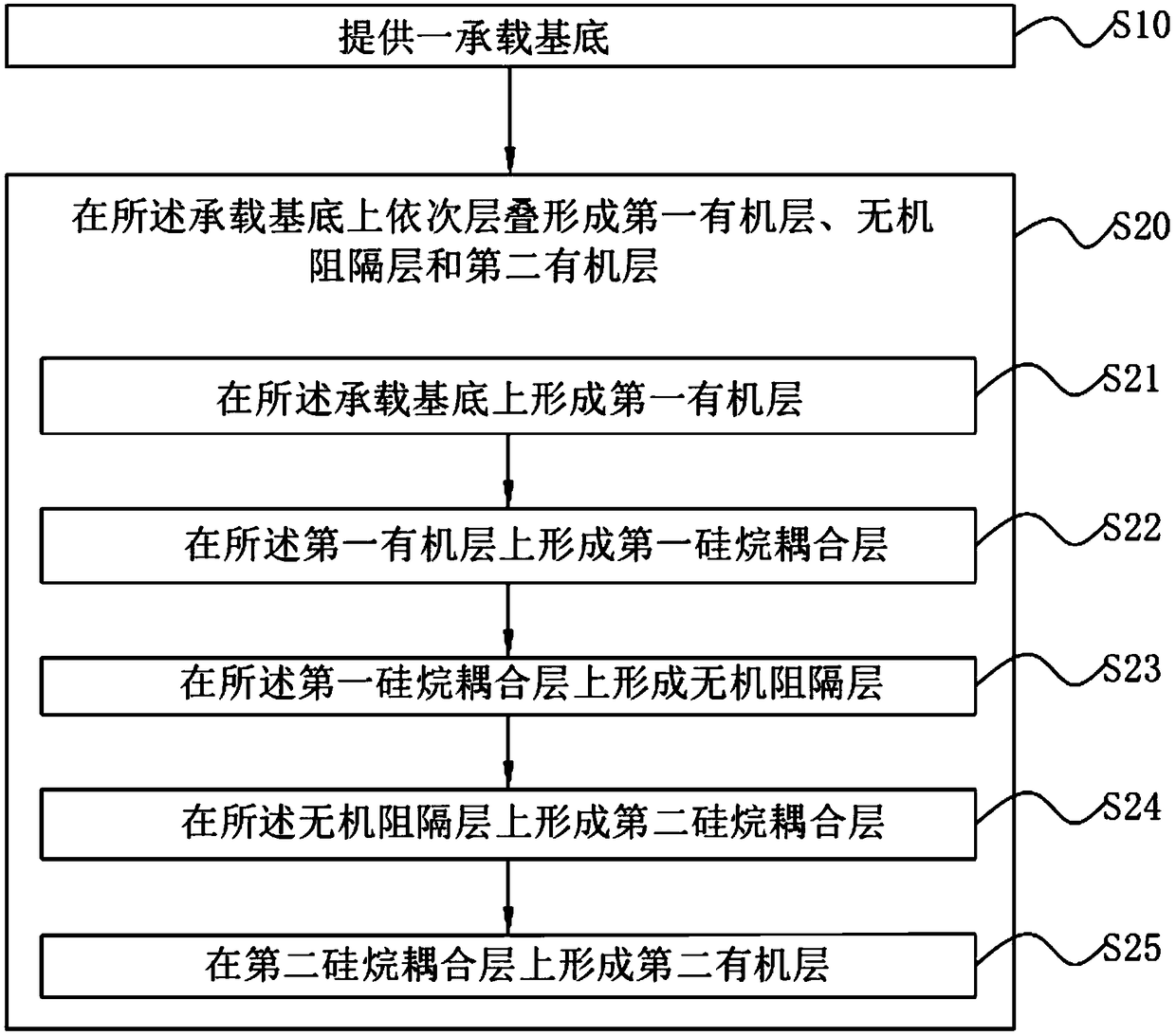
[0050] A method for preparing a display substrate, such as figure 1 Shown, described preparation method comprises:
[0051] S10, providing a bearing base;
[0052] S20, sequentially forming a first organic layer, an inorganic barrier layer and a second organic layer by laminating on the carrier substrate;
[0053] Wherein, the S20 includes:
[0054] Step S21, forming a first organic layer on the carrier substrate;
[0055] Step S22, forming a first silane coupling layer on the first organic layer;
[0056] Step S23, forming an inorganic barrier layer on the first silane coupling layer;
[0057] Step S24, forming a second silane coupling layer on the inorganic barrier layer;
[0058] Step S25, forming a second organic layer on the second silane coupling layer.
[0059] Wherein, both the first silane coupling layer and the second silane coupling layer are made of a silane coupling agent by spraying or coating. The silane coupling agent is a material containing both inorgan...
Embodiment 2
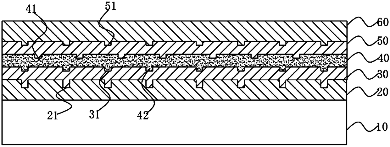
[0090] Such as Figure 4 As shown, the second groove 41 includes a plurality of grooves, and both ends of the grooves extend toward the edge of the inorganic barrier layer 40 to penetrate the inorganic barrier layer 40 . The main advantage of inorganic materials is better water and oxygen barrier performance, but compared with organic materials, inorganic materials have poor bending resistance. When the display panel is bent, the thicker inorganic film may crack or break. The second groove 41 is used as a bending stress release area when the display substrate is bent, and the inorganic film layer at the bottom of the second groove 41 is thinner, so that it can bear greater bending stress, thereby preventing inorganic barriers during the bending process of the display substrate. Layer 40 is cracked or broken.
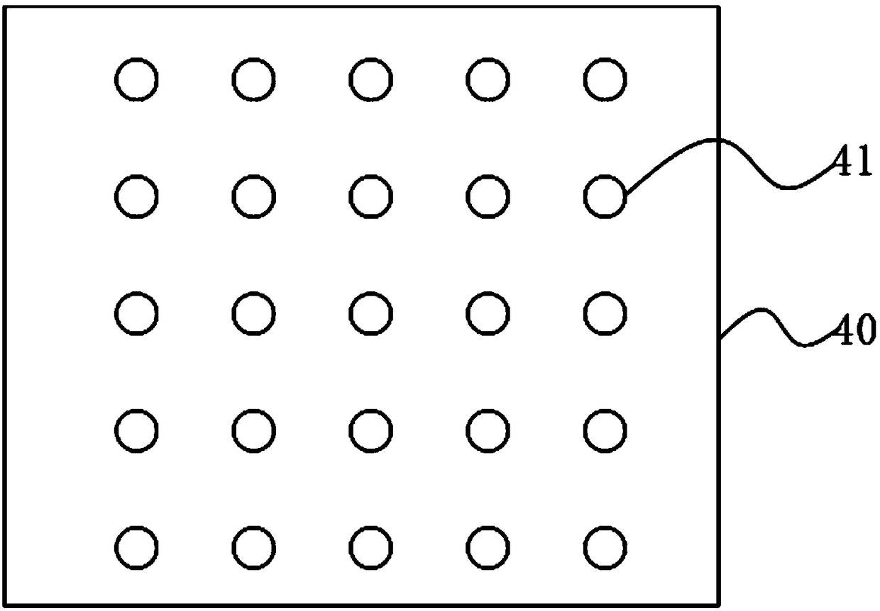
[0091] as shown in the picture Figure 5 As shown, the vertical projection of the groove does not coincide with the vertical projection of the filling block 42 . The ...
PUM
| Property | Measurement | Unit |
|---|---|---|
| Thickness | aaaaa | aaaaa |
| Thickness | aaaaa | aaaaa |
| Thickness | aaaaa | aaaaa |
Abstract
Description
Claims
Application Information
 - Generate Ideas
- Intellectual Property
- Life Sciences
- Materials
- Tech Scout
- Unparalleled Data Quality
- Higher Quality Content
- 60% Fewer Hallucinations
Browse by: Latest US Patents, China's latest patents, Technical Efficacy Thesaurus, Application Domain, Technology Topic, Popular Technical Reports.
© 2025 PatSnap. All rights reserved.Legal|Privacy policy|Modern Slavery Act Transparency Statement|Sitemap|About US| Contact US: help@patsnap.com