Organic field-effect multilevel transistor memory on basis of light regulation and control and method for preparing organic field-effect multilevel transistor memory

An organic field and light regulation technology, which is applied in the fields of organic semiconductor device materials, semiconductor/solid-state device manufacturing, and electric solid-state devices, etc., can solve the problems of potential safety hazards, large operating voltage, waste of resources, etc. The effect of reducing the dependence on operating voltage and reducing labor costs

Inactive Publication Date: 2019-02-12
CHINA INFOMRAITON CONSULTING & DESIGNING INST CO LTD
View PDF4 Cites 3 Cited by
  • Summary
  • Abstract
  • Description
  • Claims
  • Application Information

AI Technical Summary

Problems solved by technology

However, this method requires a larger operating voltage, wastes resources, an

Method used


Image

  • Organic field-effect multilevel transistor memory on basis of light regulation and control and method for preparing organic field-effect multilevel transistor memory
  • Organic field-effect multilevel transistor memory on basis of light regulation and control and method for preparing organic field-effect multilevel transistor memory
  • Organic field-effect multilevel transistor memory on basis of light regulation and control and method for preparing organic field-effect multilevel transistor memory

Examples


Embodiment 1

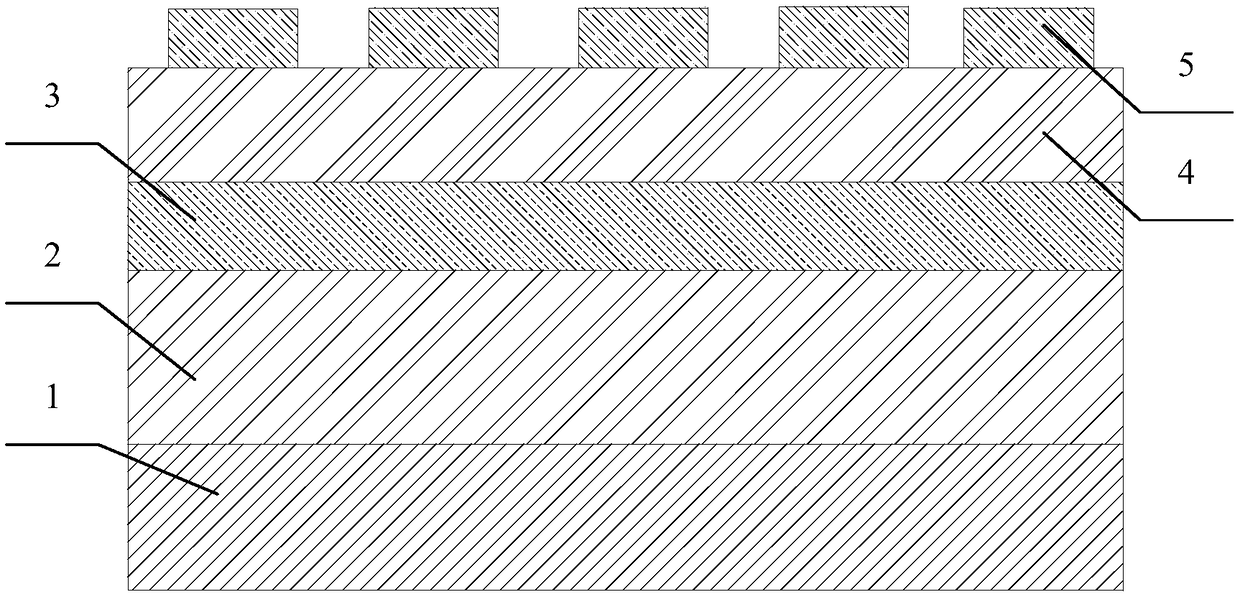
[0038] The organic field effect transistor memory structure, its structure schematic diagram is as follows figure 1 shown, including:

[0039] A substrate 1 with a gate electrode formed on its surface;

[0040] a gate insulating layer 2 covering the gate electrode;

[0041] A quantum dot-doped thin film layer 3 formed on the gate insulating layer 2;

[0042]A photosensitive semiconductor layer 4 formed on the quantum dot-doped thin film layer 3; and

[0043] The source and drain electrodes 5 are formed on both sides of the channel region on the surface of the photosensitive semiconductor layer 4 .

[0044] In the technical solution of this embodiment, a highly doped silicon wafer with a gate electrode formed on its surface is used as the substrate, and the thickness of the substrate 1 is about 650 μm (the silicon wafer is a commercial product, purchased from Suzhou Jingsi Electronic Technology Co., Ltd.); A layer of 50nm silicon dioxide is used as a gate insulating layer; ...

Embodiment 2

[0062] In the technical scheme of this embodiment, a heavily doped silicon wafer is used as a substrate, and a gate electrode is formed on the surface substrate; a layer of 300nm silicon dioxide is used as a gate insulating layer; doped with lead selenide quantum dots (PbSe) The polystyrene (PS) film is a quantum dot-doped thin film layer, its thickness is 25nm, as a charge transport layer; a layer of 30nm thick pentacene is vapor-deposited on the quantum dot-doped thin film layer as a photosensitive semiconductor layer; Metal copper is vapor-deposited on both sides of the conductive channel of the photosensitive semiconductor layer as source and drain electrodes.

[0063] During actual preparation, the room temperature in the laboratory is kept at about 25°C, and the indoor humidity is kept at about 40%.

[0064] The specific preparation steps of the memory described in this embodiment are as follows:

[0065] (1) configure lead selenide (PbSe) solution, the solution concent...


PUM

PropertyMeasurementUnit
Thicknessaaaaaaaaaa
Membrane thicknessaaaaaaaaaa
Thicknessaaaaaaaaaa

Abstract

The invention discloses an organic field-effect multilevel transistor memory on the basis of light regulation and control. The organic field-effect multilevel transistor memory sequentially comprisesa substrate, a gate insulation layer, a quantum dot doped thin film layer, a photosensitive semiconductor layer and source and drain electrodes from bottom to top. The source and drain electrodes areformed on the photosensitive semiconductor layer; the quantum dot doped thin film layer is a polymer thin film with doped semiconductor nanometer crystals. The organic field-effect multilevel transistor memory has the advantages that the memory properties and the photosensitivity of devices can be improved by the aid of simple technological means, accordingly, the memory capacity and the photo-responsiveness of the devices can be greatly enhanced, the switch speeds of the devices can be greatly increased, and multilevel memory can be implemented, the preparation costs of the devices further can be reduced, and accordingly popularization and application can be facilitated.

Description

technical field [0001] The invention belongs to the field of memory technology and light detection technology in the semiconductor industry, and specifically relates to an organic field effect multi-stage transistor memory based on light control and a preparation method thereof. Background technique [0002] In the context of today's hot big data era, the rapid development of information technology has put forward higher requirements for data storage, such as storage speed, storage density, component size, mechanical flexibility, manufacturing process, and price and cost. The development trend of organic field effect transistor memories with high performance meets the above requirements. A large number of researchers start with the device structure of the organic field effect transistor memory, the material of each functional layer of the device, and the morphology of the film to control the performance of the organic field effect transistor memory. [0003] In recent years...

Claims


Application Information

Patent Timeline
IPC IPC(8): H01L51/05H01L51/10H01L51/56H01L51/54
CPCH10K85/00H10K10/46H10K10/20H10K10/80H10K2102/00H10K71/00
Inventor 李焕群周楠魏贤虎王睿
Owner CHINA INFOMRAITON CONSULTING & DESIGNING INST CO LTD
Why Eureka
Try Eureka