
Semiconductor device cleaning process and device

A technology for cleaning devices and semiconductors, used in cleaning methods using liquids, chemical instruments and methods, cleaning methods and utensils, etc., can solve the problems of large consumption of acetone and IPA, long cleaning time, serious volatilization, etc., to remove residues Organic matter, good cleaning effect, pollution reduction effect

Inactive Publication Date: 2019-02-15
YANGZHOU HY TECH DEV
View PDF7 Cites 3 Cited by
  • Summary
  • Abstract
  • Description
  • Claims
  • Application Information

AI Technical Summary

Problems solved by technology

[0003] At present, the cleaning method used in the industry is a mixed solution of acetone and IPA. The disadvantages of this cleaning method are poor cleaning power, long cleaning time, serious volatilization, and high consumption of acetone and IPA.

Method used


Image

  • Semiconductor device cleaning process and device
  • Semiconductor device cleaning process and device

Examples


Embodiment Construction

[0031] In order to make the object, technical solution and advantages of the present invention clearer, the present invention will be further described in detail below in conjunction with specific embodiments.

[0032] It should be noted that, in the case of no conflict, the embodiments in the present application and the features in the embodiments can be combined with each other.

[0033] The raw materials and equipment used in the following examples are commercially available unless otherwise specified.

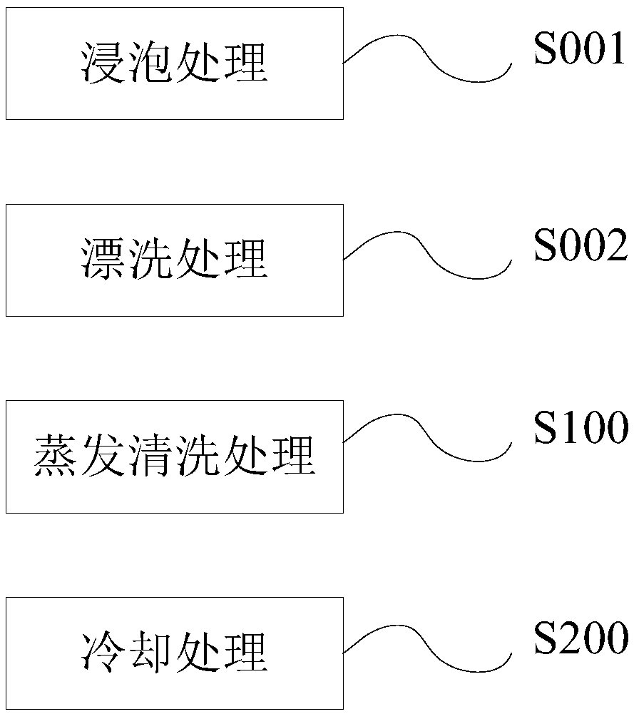
[0034] see figure 1 , the present invention provides a semiconductor device cleaning process, which comprises the following steps:

[0035] S100: evaporative cleaning step; use n-bromopropane vapor to clean the semi-conductor device to be treated; usually, the cleaning agent n-bromopropane solvent is heated to evaporate, and then the semiconductor device is placed in n-bromopropane vapor, at this time the n-bromopropane Propane vapor can completely cover the entire surfac...


PUM


Abstract

The invention provides a semiconductor device cleaning process. The process comprises the following steps that S100, evaporating and cleaning are carried out, the semiconductor device to be treated iswashed by using a normal-bromine propane steam; S200, condensing is carried out, a condensation device is adopted for condensation treatment, so that the normal-bromine propane steam can be condensedinto liquid drops on a semiconductor device body; and the invention further provides a semiconductor cleaning device, specifically comprises an evaporative-condensation washing device, wherein the steam-condensation washing device comprises a closed shell body, a heating groove, a first heating device, a supporting frame and a condensing device. According to the process and the device, an evaporation-condensation process is adopted to realize repeated use of a cleaning agent, so that the cost is reduced, and the pollution is reduced.

Description

technical field [0001] The invention relates to the field of semiconductor device processing, in particular to a cleaning process and device for semiconductor devices obtained after soldering processing. Background technique [0002] At present, after the soldering of semiconductor devices is completed, various residues (such as flux, impurities, carbides, etc.) will exist on the surface of the devices. Since the flux is weakly acidic, long-term use will corrode the welding plate and the grain itself, and the reliability and stability of the semiconductor material itself will be reduced; while impurities and carbides will increase the leakage of the material, resulting in high-temperature characteristics of the material. Reduction, especially in the high failure rate of high temperature leakage current test items. Therefore, it is necessary to clean the surface of the semiconductor device. [0003] The current method used in the industry is acetone and IPA mixed solution c...

Claims


Application Information

Patent Timeline
Patent Type & Authority Applications(China)
IPC IPC(8): B08B3/02B08B3/08B08B3/10B08B3/04
CPCB08B3/02B08B3/04B08B3/08B08B3/10
Inventor 高定健
Owner YANGZHOU HY TECH DEV
Learn More