A multi-channel multi-mode multiplexing waveguide intersection and its preparation method

A multi-mode, multi-channel technology, applied in the direction of optical waveguide light guide, light guide, instrument, etc., can solve the problems of small breakthrough, hinder application, increase the transmission capacity of communication system, etc., achieve low loss, reduce loss, and low crosstalk Effect

Active Publication Date: 2020-07-10
SOUTH CENTRAL UNIVERSITY FOR NATIONALITIES
View PDF10 Cites 0 Cited by
  • Summary
  • Abstract
  • Description
  • Claims
  • Application Information

AI Technical Summary

Problems solved by technology

However, the mode splitting ability of the Y-shaped structure is limited and cannot support other higher-order TE modes
[0004] In summary, the existing dual-waveguide crossover structure only supports two waveguide modes and two crossover channels, which severely limits the density and capacity of the multimode routing system, and the dual-mode waveguide crosspoint is difficult to expand and support more modes or More channels, greatly hindering their application in future high-density multimode routing solutions
In addition, the traditional waveguide intersection design method only relies on the design of the device shape, and the breakthrough is small. Therefore, increasing the waveguide mode and cross channel of the optical waveguide is particularly critical to increase the transmission capacity of the communication system.

Method used


Image

  • A multi-channel multi-mode multiplexing waveguide intersection and its preparation method
  • A multi-channel multi-mode multiplexing waveguide intersection and its preparation method
  • A multi-channel multi-mode multiplexing waveguide intersection and its preparation method

Examples


Embodiment 1

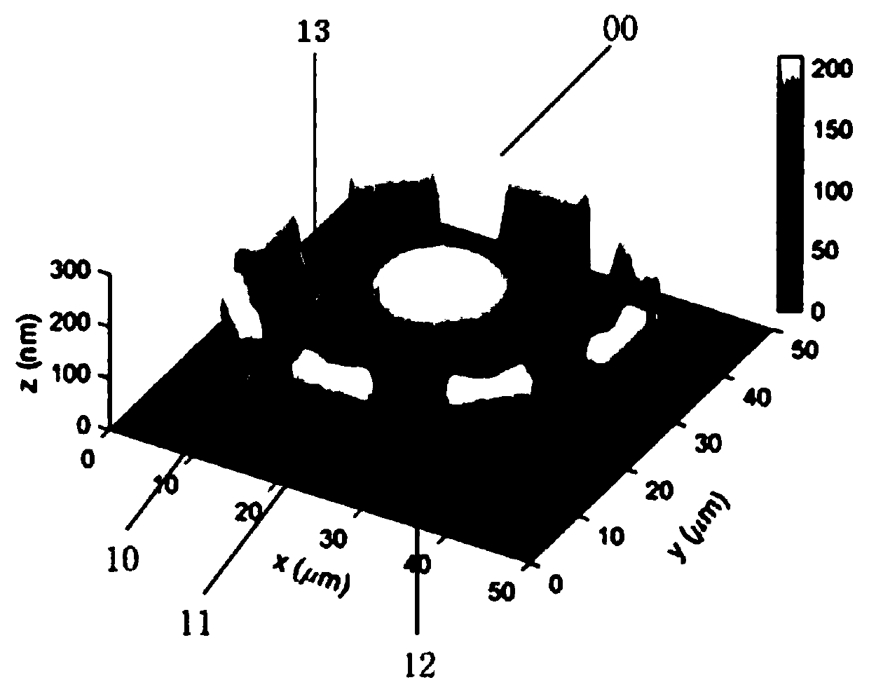
[0079] 1. Embodiment 1: Four-channel third-order mode waveguide crossover

[0080] 1) specific size

[0081] The multi-channel multi-mode multiplexing waveguide cross is Si material, using a new semi-analytic artificial boundary conformal mapping method, combined with Laplace equation and finite element method, the calculation is obtained:

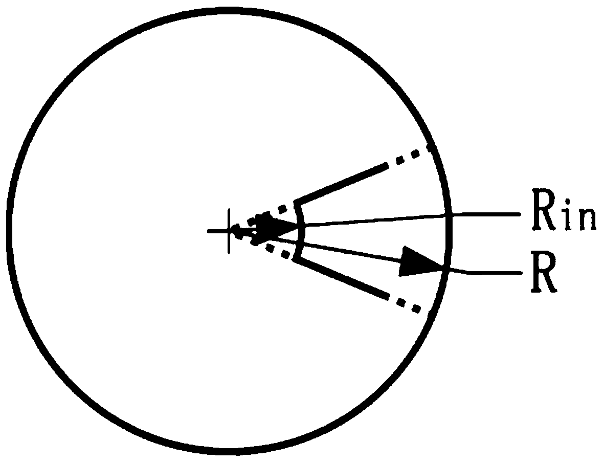
[0082] Multi-channel multi-mode multiplexing waveguide intersection radius R is 25μm, R in 3 μm;

[0083] The refractive index of the multi-channel multi-mode multiplexing waveguide cross center is 2.83;

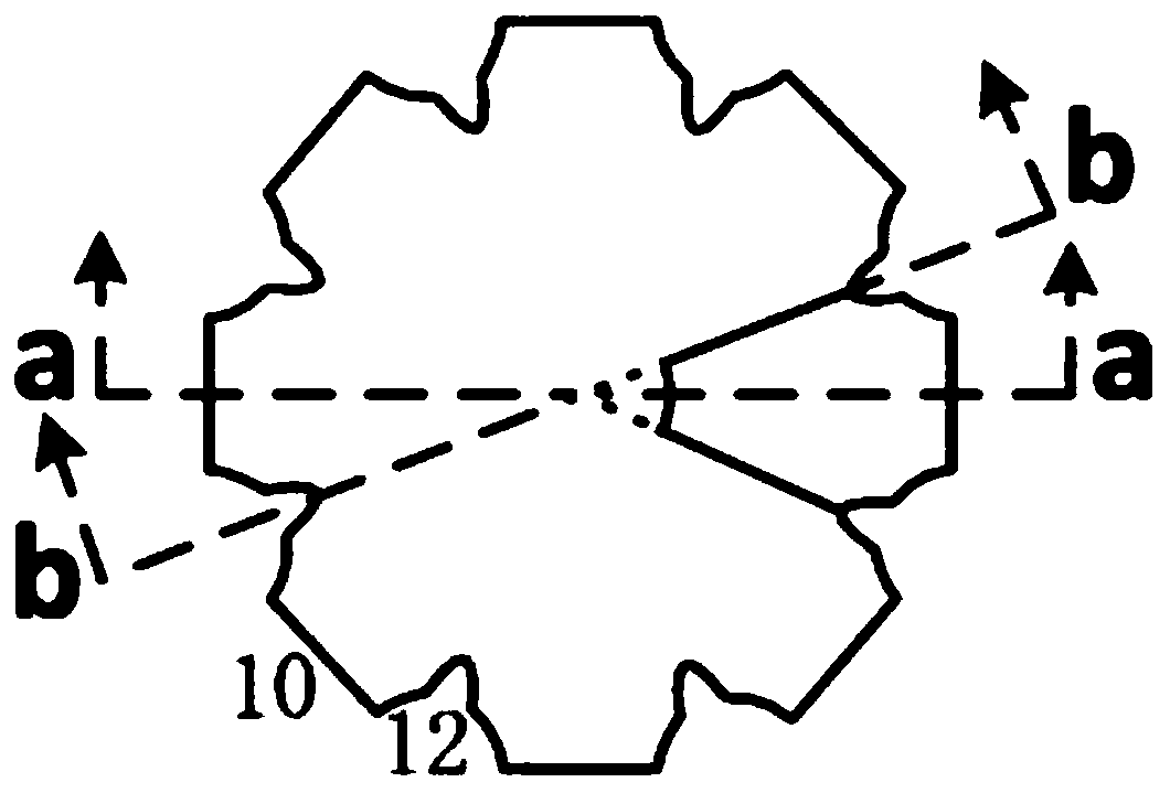
[0084] The plane boundary 11 has a refractive index of 2.83, a height of 220 nm, and a width of 8.77 μm;

[0085] The horizontal length of the third-order Bezier curve of the curved boundary 12 is 6.05 μm;

[0086] The radial length from the center to the beginning of the third-order Bezier curve is 16.9 μm;

[0087] The refractive index distribution of the multi-channel and multi-mode multiplexing waveguide cross-curved waveguide 1...


PUM


Abstract

The invention discloses a multichannel multimode multiplexed waveguide crossover and a preparation method thereof, and relates to waveguide crossovers of photon integration technology. The waveguidecrossover is a special-shaped silicon cylinder (00), and comprises 2N centrally symmetric ports (10), wherein N is a natural number, 2<=N<=100. A planar boundary (11) is arranged at the outer wall ofeach port (10). A curved boundary (12) is arranged between adjacent ports (10). A surface boundary (13) is arranged on the inner side to the center of each port (10). According to the waveguide crossover and the preparation method thereof, the waveguide crossover of three channels or above can be realized; the high-order mode multiplexing can be achieved at the same time; and the dense integrationon a chip can be realized. The working bandwidth is extremely wide, the loss and the crosstalk are small.

Description

technical field [0001] The invention relates to a waveguide intersection of photon integration technology, in particular to a multi-channel multi-mode multiplexing waveguide intersection and a preparation method thereof. Background technique [0002] As high-speed optical communication moves towards the 200G / 400G era, the challenges of data center optical interconnection to bandwidth, density, power consumption, cost and delay drive the development of photonic integration technology. Photonic integration has the advantages of small size and low power consumption. It is a key technology to solve the problems of energy consumption, volume and capacity of optical interconnection in future broadband optical networks. SOI is a silicon material used for large-scale integrated optical circuits. It has attracted people's attention because of its superior optical properties and the manufacture of silicon-based optical devices that are compatible with CMOS processes and are easy to ac...

Claims


Application Information

Patent Timeline
Patent Type & Authority Patents(China)
IPC IPC(8): G02B6/125G02B6/13G02B6/136G02B27/00
CPCG02B6/125G02B6/13G02B6/136G02B27/0012
Inventor 侯金李书轶郜定山陈焕阳杨春勇陈少平陶伟
Owner SOUTH CENTRAL UNIVERSITY FOR NATIONALITIES
Why Eureka
Try Eureka