Beam splitting laser cutting method for silicon carbide based wafers

A laser cutting, silicon carbide-based technology, applied in laser welding equipment, welding equipment, metal processing equipment, etc., to achieve the effect of eliminating wafer chipping, reducing the width of the cut mark, and improving accuracy

Active Publication Date: 2019-02-19
SHENZHEN STS MICROELECTRONICS
View PDF10 Cites 6 Cited by
  • Summary
  • Abstract
  • Description
  • Claims
  • Application Information

AI Technical Summary

Problems solved by technology

However, the patent document TWI628027B has no step-by-step cutting technolo

Method used


Image

  • Beam splitting laser cutting method for silicon carbide based wafers
  • Beam splitting laser cutting method for silicon carbide based wafers
  • Beam splitting laser cutting method for silicon carbide based wafers

Examples


Embodiment Construction

[0046] Hereinafter, the present invention will be further described with reference to the drawings and specific embodiments.

[0047] First describe the conceptual design of the present invention as follows:

[0048] 1. Brief introduction of cutting process

[0049] Film application steps:

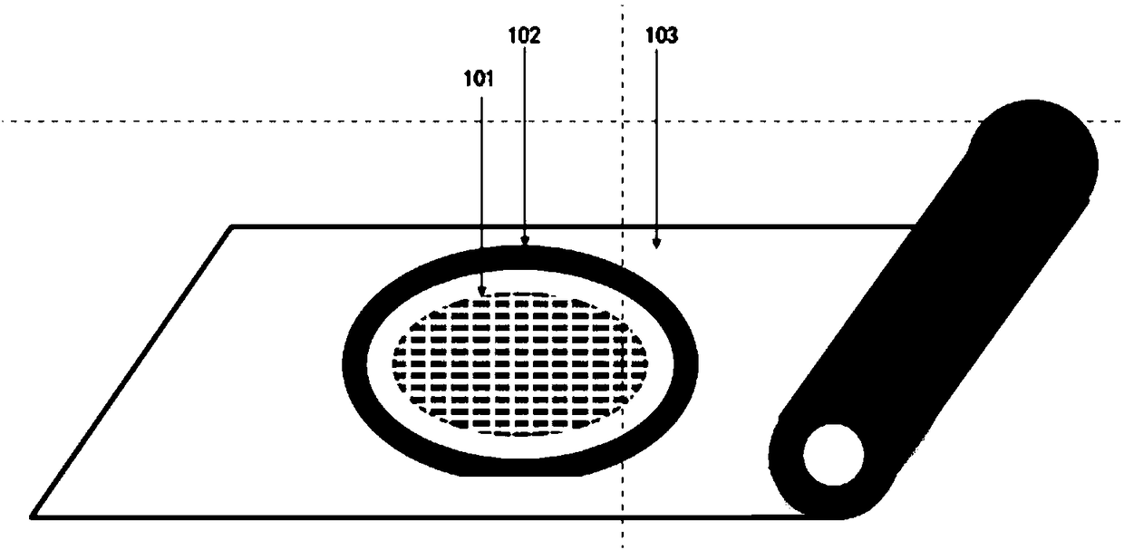
[0050] Such as figure 1 As shown, the silicon-based wafer 101 and the iron ring 102 are pasted on the film 103, the film part outside the iron ring 102 is scratched off with a blade, and the film part inside the iron ring 102 is retained.

[0051] Purpose: to paste the silicon-based wafer 101 on the film 103 and fix it with the iron ring 102, which is convenient for processing, cutting and patching.

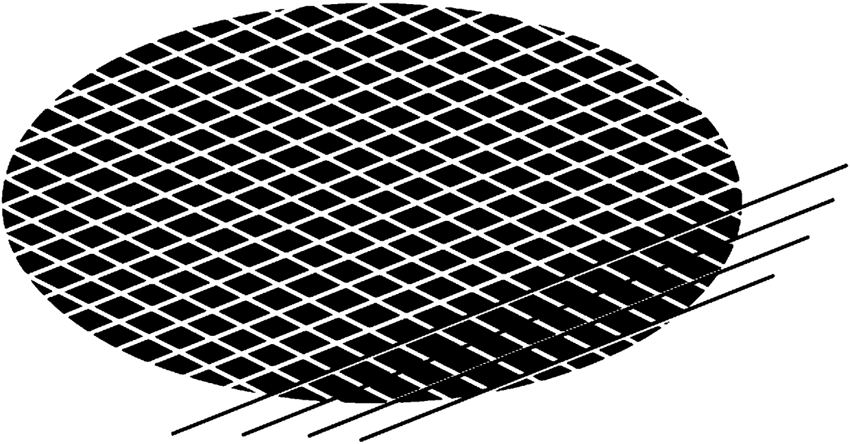
[0052] Cutting steps:

[0053] Such as figure 2 As shown, the wafer is cut one or more times in a certain cutting mode according to a certain cutting pattern, such as depth, speed, position, and width.

[0054] Purpose: to divide the entire wafer into independent, functional chips ...


PUM


Abstract

The invention discloses a beam splitting laser cutting method for silicon carbide based wafers, and the method is used for cutting silicon carbide based wafers into independent chips. The beam splitting laser cutting method for silicon carbide based wafers is characterized by comprising the following steps: pretreatment step; diffraction light splitting step: using an optical grating device (106)to split single-beam laser (105) into multi-beam laser (108) and forming beam patterns; beam splitting cutting step: using a laser cutter to cut silicon carbide based wafers; and after treatment step.The beam splitting laser cutting method for silicon carbide based wafers achieves the technical effects of improving the cutting rate of wafers and at the same time improving the cutting quality of wafers.

Description

technical field [0001] The invention relates to the technical field of laser beam cutting, wherein the beam is divided into multiple beams (B23K26 / 067), and a mask is used to form the pattern shape of the laser beam (B23K 26 / 06). Wafer split laser cutting method. Background technique [0002] Smart devices have developed rapidly in recent years, and people's requirements for smart devices are also developing in the direction of multi-function, precision, and high integration. This kind of demand also puts forward small, thin and light process requirements for electronic components, as well as performance requirements for ultra-low energy consumption, fast heat dissipation, and high amplification efficiency. [0003] Due to the impact of small, thin, and lightweight chips, the traditional wafer blade cutting process has gradually shown a decline in chip cutting speed and reliability, and has been gradually eliminated by changing market demand. Due to its faster cutting spee...

Claims


Application Information

Patent Timeline
IPC IPC(8): B23K26/38B23K26/402B23K26/067B23K26/02B23K26/70
CPCB23K26/02B23K26/0673B23K26/38B23K26/402B23K26/70
Inventor 詹苏庚吴迪彭立和王红丁锋
Owner SHENZHEN STS MICROELECTRONICS
Why Eureka
Try Eureka