

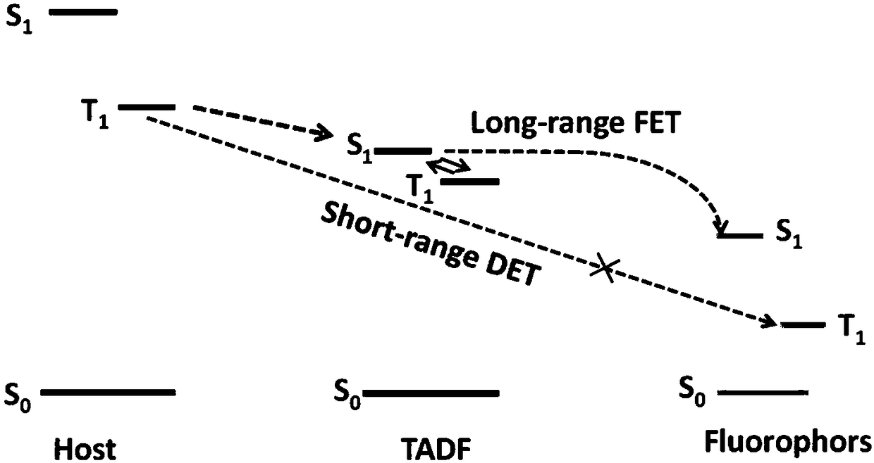
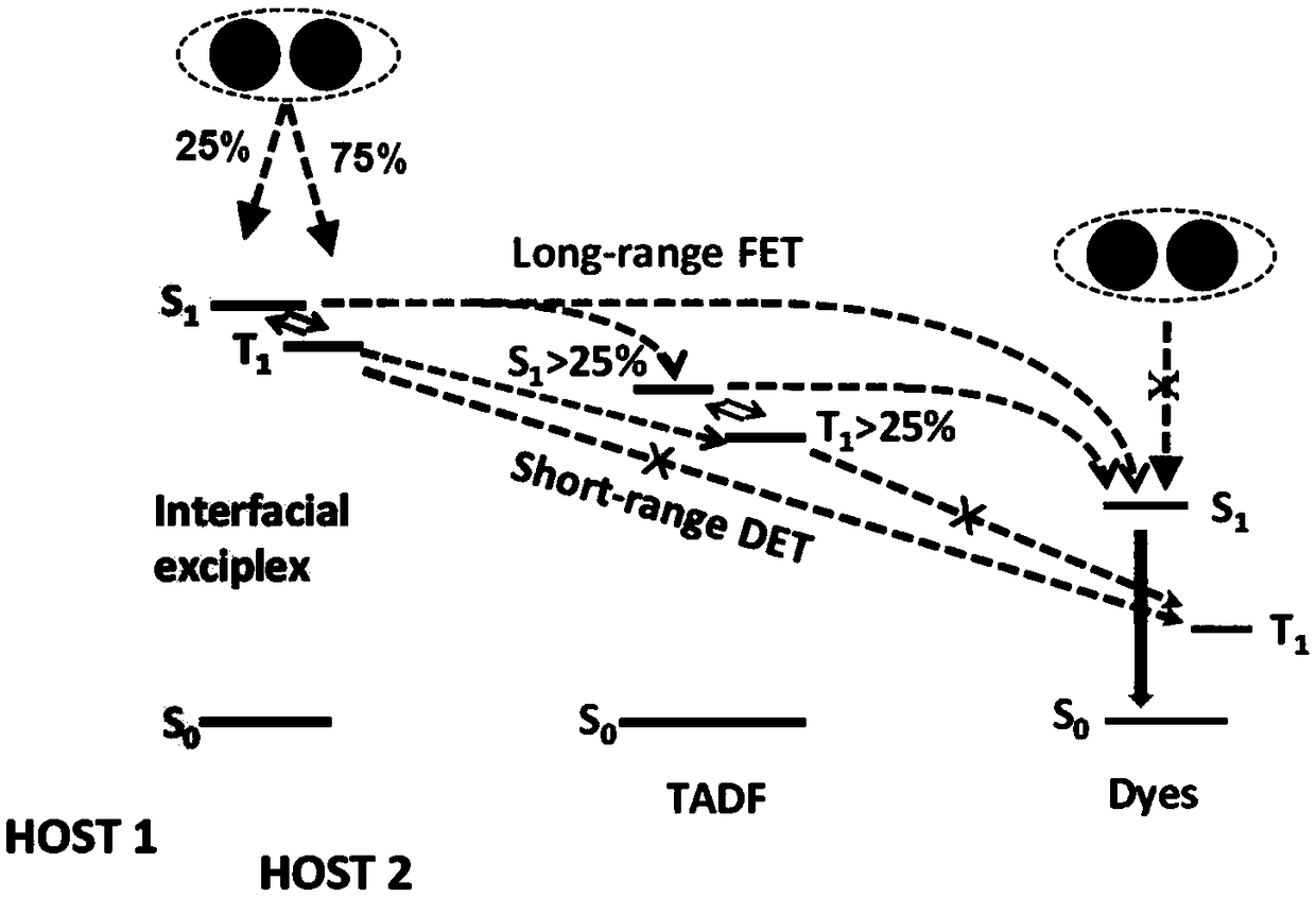
Organic electroluminescent device and display device
An electroluminescent device and electroluminescent technology, which are applied in electric solid devices, electrical components, semiconductor devices, etc., can solve the problems of poor color purity, high exciton concentration, efficiency roll-off, etc., and improve the exciton utilization rate. , widening the composite area, reducing the effect of efficiency roll-off
- Summary
- Abstract
- Description
- Claims
- Application Information
AI Technical Summary
Problems solved by technology
Method used
Image

Examples
Embodiment 1
[0078] The glass plate coated with the ITO transparent conductive layer was ultrasonically treated in a commercial cleaning agent, rinsed in deionized water, ultrasonically degreased in acetone: ethanol mixed solvent, baked in a clean environment until the water was completely removed, and treated with ultraviolet light. and ozone cleaning, and bombard the surface with a low-energy positive ion beam;
[0079] Place the above-mentioned glass substrate with the anode in a vacuum chamber and evacuate to 1×10 -5 ~9×10 -3Pa, the compound HI-2 was vacuum-evaporated on the above-mentioned anode layer as a hole injection layer, the evaporation rate was 0.1nm / s, and the evaporation film thickness was 10nm;
[0080] The compound HT-28 was vacuum evaporated on the surface of the hole injection layer as the hole transport layer of the device, the evaporation rate was 0.1nm / s, and the total film thickness was 40nm;
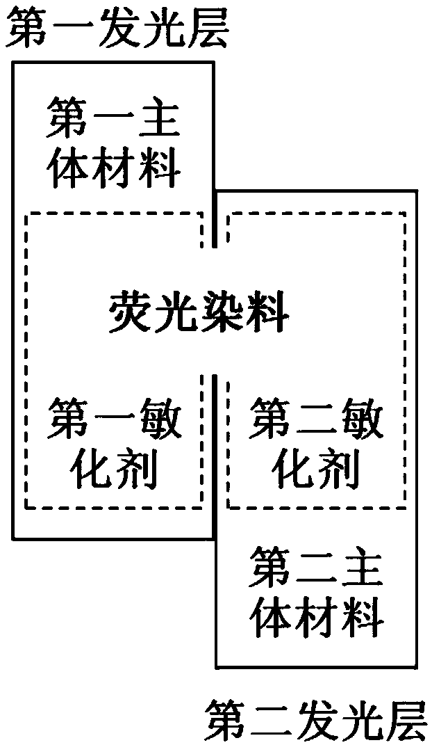
[0081] The first light-emitting layer of the device is vacuum-evaporate...
Embodiment 2~5
[0090] The preparation method of the organic electroluminescent device in Examples 2 to 5 is basically the same as that of Example 1, the only difference is that the material selection, doping concentration and / or thickness of the first light-emitting layer and the second light-emitting layer are different, specifically the first The materials, doping concentrations and thicknesses used for the light-emitting layer and the second light-emitting layer are shown in Table 3, and the materials and thicknesses of other functional layers are shown in Table 2.
[0091] Material, doping concentration and thickness of OLED device light-emitting layer in Table 3 Examples 2-5
[0092]
[0093] In Examples 2 to 5, the first sensitizer and the second sensitizer are different, and the first dye and the second dye are the same; for the specific structures of the first light-emitting layer and the second light-emitting layer, please refer to image 3 .
Embodiment 6~10
[0095] The preparation method of the organic electroluminescent device in Examples 6-10 is basically the same as that of Example 1, the only difference lies in the material selection, doping concentration and / or thickness of the first light-emitting layer and the second light-emitting layer. Specifically, the materials, doping concentrations and thicknesses used in the first light-emitting layer and the second light-emitting layer are shown in Table 4, and the materials and thicknesses of other functional layers can be found in Table 2.
[0096] Material, doping concentration and thickness of OLED device light-emitting layer in Table 4 Examples 6-10
[0097]
[0098] In Examples 6-10, the first dye and the second dye are different, and the specific structure of the first light-emitting layer and the second light-emitting layer in the OLED device can refer to Figure 4 .
PUM
| Property | Measurement | Unit |
|---|---|---|
| Thickness | aaaaa | aaaaa |
| Thickness | aaaaa | aaaaa |
Abstract
Description
Claims
Application Information