Pre-cleaning cavity and semiconductor processing device

A pre-cleaning and chamber technology, which is applied in the field of pre-cleaning chambers and semiconductor processing equipment, can solve the problems of reducing product yield and wafer surface contamination, so as to improve yield, reduce metal ion pollution, and weaken radial electric field strength Effect

Active Publication Date: 2019-02-26
BEIJING NAURA MICROELECTRONICS EQUIP CO LTD
View PDF8 Cites 4 Cited by
  • Summary
  • Abstract
  • Description
  • Claims
  • Application Information

AI Technical Summary

Problems solved by technology

Under the action of high-energy ions, the surface of the metal plate 160 will be bombarded to produce aluminum ions or aluminum atoms, and part of the produced aluminum ions or aluminum atoms will reach the surface of the wafer through the first air hole 161 in the metal plate 160 and adhere, thereby Causes contamination on the wafer surface and reduces product yield

Method used


Image

  • Pre-cleaning cavity and semiconductor processing device
  • Pre-cleaning cavity and semiconductor processing device
  • Pre-cleaning cavity and semiconductor processing device

Examples


Embodiment Construction

[0050] Specific embodiments of the present invention will be described in detail below in conjunction with the accompanying drawings. It should be understood that the specific embodiments described here are only used to illustrate and explain the present invention, and are not intended to limit the present invention.

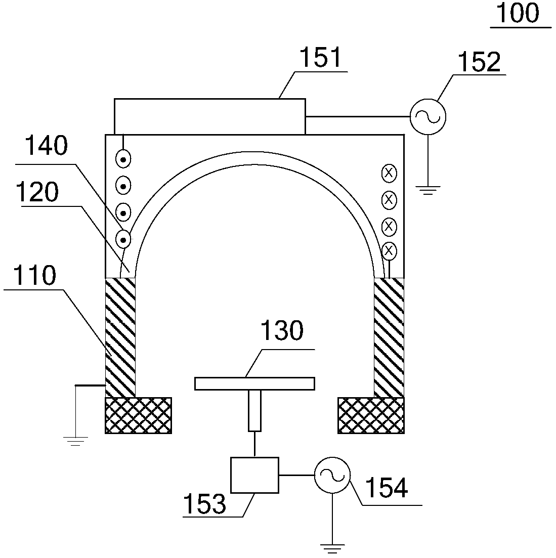
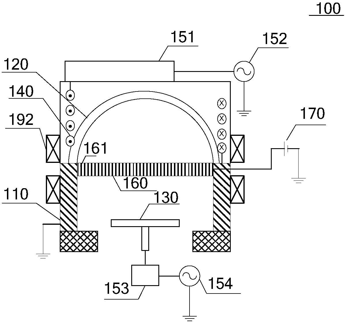
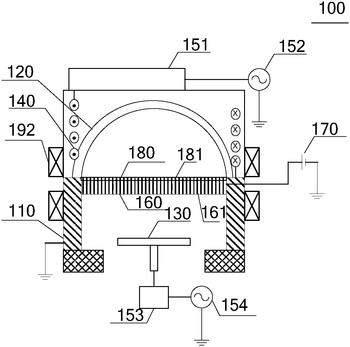
[0051] Such as image 3 , Figure 4 with Figure 5 As shown, the first aspect of the present invention relates to a pre-cleaning chamber 100 . The pre-cleaning chamber 100 mainly includes a cavity 110, a top cover 120, a carrier 130, an inductance coil 140, a first radio frequency matching device 151, a first radio frequency power source 152, a second radio frequency matching device 153 and a second radio frequency power source 154 . Wherein, the top cover 120 is disposed on the top of the cavity 110 , that is, the top cover 120 is disposed on the top of the cavity 110 to enclose a sealed space together with the cavity 110 . The cavity 110 can be columnar, ...


PUM


Abstract

The present invention discloses a pre-cleaning cavity and a semiconductor processing device. The pre-cleaning cavity comprises a cavity, a top cover, a bearing piece and a metal plate. The top cover is arranged at the top end of the cavity and is configured to seal the cavity, the bearing piece is arranged at the bottom portion of the cavity and configured to bear a wafer, the metal plate is horizontally arranged between the bearing piece and the top cover and is provided with a plurality of first vent holes penetrating the thickness of the metal plate, the metal plate is earthed to filter outions in plasmas, the plasmas form a plasma sheath at the surface of the metal plate, the pre-cleaning cavity further comprises an insulation protection plate arranged between the metal plate and thetop cover, the insulation protection plate is provided with a plurality of second vent holes penetrating the thickness of the insulation protection plate, and the insulation protection plate can prevent ions from bombarding the surface of the metal plate under the drive of the voltage of the plasma sheath. The pre-cleaning cavity can effectively reduce the metal ion pollution of the surface of thewafer and can improve the yield of the wafer cleaning.

Description

technical field [0001] The invention relates to the technical field of semiconductor manufacturing, in particular to a pre-cleaning chamber and semiconductor processing equipment comprising the pre-cleaning chamber. Background technique [0002] Plasma equipment is widely used in today's semiconductor integrated circuits, solar cells, flat panel displays and other manufacturing processes. Plasma processing equipment that has been widely used in the industry includes the following types: for example, DC discharge type, capacitively coupled (CCP) type, inductively coupled (ICP) type, and electron cyclotron resonance (ECR) type. These types of plasma processing equipment are currently used in processes such as physical vapor deposition (PVD), plasma etching, plasma chemical vapor deposition (CVD), and cleaning. [0003] During the process, in order to improve the quality of the product, before implementing the deposition process, the wafer should be pre-cleaned (Preclean) to r...

Claims


Application Information

Patent Timeline
Patent Type & Authority Applications(China)
IPC IPC(8): H01J37/32
CPCH01J37/32504H01J2237/335Y02P70/50
Inventor 姜鑫先陈鹏
Owner BEIJING NAURA MICROELECTRONICS EQUIP CO LTD
Why Eureka
Try Eureka