Chip on glass package assembly

一种封装组件、玻璃芯片的技术,应用在电气元件、电固体器件、半导体器件等方向,能够解决成本昂贵、触控显示器成本增加、柔性电路板设计和布局复杂等问题,达到降低生产成本的效果

Active Publication Date: 2019-03-01
NOVATEK MICROELECTRONICS CORP
View PDF5 Cites 1 Cited by
  • Summary
  • Abstract
  • Description
  • Claims
  • Application Information

AI Technical Summary

Problems solved by technology

However, the design and layout of such a flexible circuit board are complicated, and the cost of electrical testing of the electronic device on the flexible circuit board is expensive, resulting in an increase in the cost of the touch display

Method used


Image

  • Chip on glass package assembly
  • Chip on glass package assembly
  • Chip on glass package assembly

Examples


Embodiment Construction

[0054] Reference will now be made in detail to the exemplary embodiments of the present invention, examples of which are illustrated in the accompanying drawings. In addition, wherever possible, the same reference numerals represent the same or similar parts in the drawings and the embodiments.

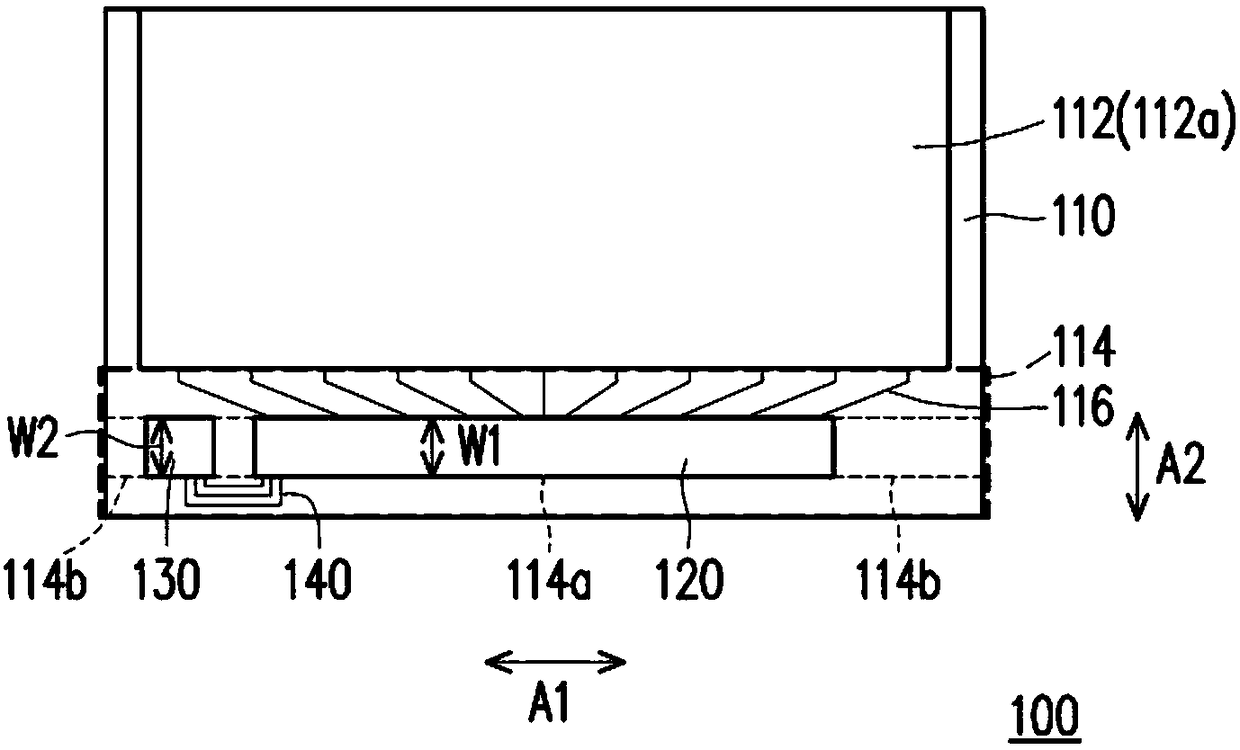
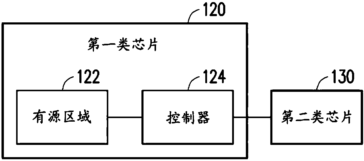
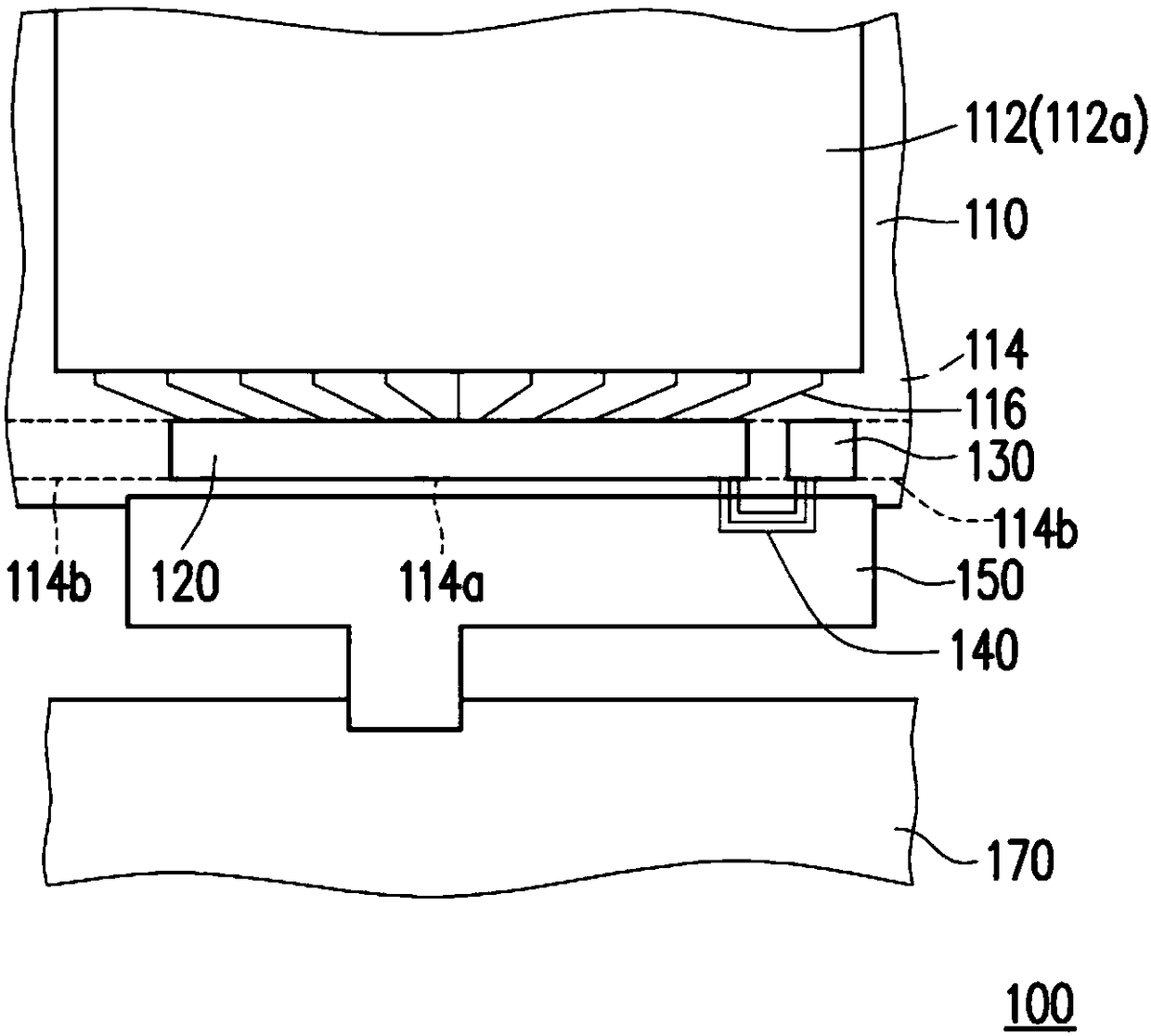
[0055] figure 1 It is a partial top view of a chip on glass (COG) package assembly according to an exemplary embodiment. figure 2 is a block diagram of a glass die bonding package assembly according to an exemplary embodiment. Please refer to figure 1 and figure 2 , in this embodiment, the glass die bonding package assembly 100 can be a touch display panel. The glass die bonding package assembly 100 includes a glass substrate 110 , a first type chip 120 , a second type chip 130 and a plurality of connecting wires 140 . The glass substrate 110 includes an active region 112 and a peripheral region 114 connected to the active region 112 . In this embodiment, the glass substrate 1...


PUM


Abstract

A chip on glass package assembly includes a glass substrate, a first type chip, a second type chip and a plurality of connecting lines. The glass substrate includes an active area and a peripheral area connected to the active area. The first type chip is mounted on the peripheral area and including a processor. The second type chip is mounted on the peripheral area and located on a side of the first type chip, wherein the second type chip is different from the first type chip. The connecting lines are disposed on the peripheral area and connecting the first type chip and the second type chip.

Description

technical field [0001] The present invention relates to a chip package, and in particular to a chip on glass (COG) package assembly. Background technique [0002] In recent years, touch display technology has been widely used in various multimedia electronic products, especially portable mobile products, such as mobile phones, electronic books (E-books), tablet computers, and so on. By using touch display technology as an input method, it can effectively replace the input method using a keyboard or mouse. In addition to convenience, touch input technology has become a widely used interaction method between human-machine interface and multimedia due to its intuitive operation characteristics. [0003] Generally speaking, the touch display panel is electrically connected to the driving device through the circuit board, so that the signal of the touch display panel can be transmitted to the driving device. In addition, a flexible printed circuit board is arranged on it, which...

Claims


Application Information

Patent Timeline
Patent Type & Authority Applications(China)
IPC IPC(8): H01L27/12H01L23/48
CPCH01L23/48H01L27/1214H05K1/147H01L25/18H05K1/148H01L23/544H01L2223/54426H01L2223/5442H01L2223/54473H01L2924/1434H01L23/5387H01L2224/13144H01L2224/02166H01L2224/13015H01L2224/13019H01L2224/11462H01L2224/1147H01L2924/00014H01L24/11H01L24/13H01L2224/0401H01L2924/15788H01L2224/8113H01L24/81H01L24/16H01L2224/16225H01L2924/00012H01L2224/05599H01L23/5386H01L24/06H01L23/49811H01L2224/16227H01L2224/06134H01L2224/05014H01L2924/1426H01L2924/14H01L2224/81129
Inventor 麦威国黄巧伶
Owner NOVATEK MICROELECTRONICS CORP
Why Eureka
Try Eureka