Multi-step deposition-based efficient crystalline silicon heterojunction solar cell electrode structure and preparation method thereof

A solar cell, multi-step deposition technology, applied in the direction of circuits, photovoltaic power generation, electrical components, etc., can solve the problems of many dangling bond defects in the intrinsic layer of amorphous silicon, less H atom content, and reduce the density of interface defect states, etc., to achieve Improve the photoelectric conversion efficiency, increase the H atom content, and reduce the effect of defect state density

Pending Publication Date: 2019-03-01
SUZHOU AIKANG LOW CARBON TECH INST
View PDF0 Cites 13 Cited by
  • Summary
  • Abstract
  • Description
  • Claims
  • Application Information

AI Technical Summary

Problems solved by technology

The existing technology is to directly deposit the P layer and the N layer after the deposition of the intrinsic layer of amorphous silicon. The content of H atoms in the directly deposited intrinsic thin layer of amorphous silicon is small, and the intrinsic layer of amorphous silicon has many dangling bond defects. , neither can effectively passivate the dangling bonds on the surface of crystalline silicon, reduce the density of interface defect states, and because of its own dangling bond defects, it will have a negative impact on the electrical properties of HJT solar cells, which cannot meet the needs of high-efficiency HJT solar cells, and cannot Further improve the photoelectric conversion efficiency of solar cells

Method used


Image

  • Multi-step deposition-based efficient crystalline silicon heterojunction solar cell electrode structure and preparation method thereof
  • Multi-step deposition-based efficient crystalline silicon heterojunction solar cell electrode structure and preparation method thereof

Examples


Embodiment 1

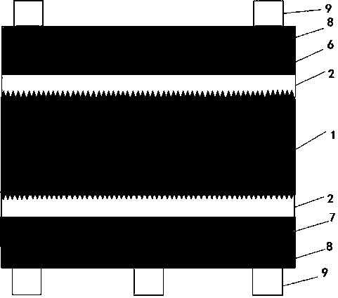
[0030] see figure 2 , the present invention relates to a multi-step deposition high-efficiency crystalline silicon heterojunction solar cell electrode structure, which includes an N-type crystalline silicon wafer 1, and the front and back sides of the N-type crystalline silicon wafer 1 are provided with two layers of amorphous Intrinsic silicon layer, that is, the first intrinsic layer 2 of amorphous silicon and the second intrinsic layer 4 of amorphous silicon are provided on the front and back sides of the N-type crystalline silicon wafer 1;

[0031] An n-type amorphous silicon doped layer 6 is provided on the outside of the second layer 4 of the intrinsic layer of amorphous silicon on the front side, and a TCO conductive film 8 is provided on the outside of the n-type amorphous silicon doped layer 6. A number of Ag electrodes 9 are provided on the outside of the front TCO conductive film 8;

[0032] A p-type amorphous silicon doped layer 7 is provided outside the second l...

Embodiment 2

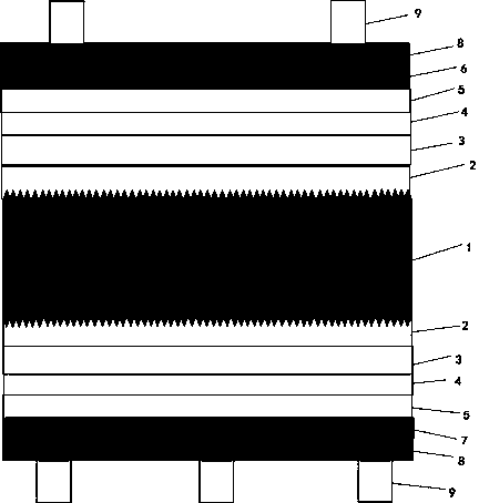
[0046] see figure 2 , the present invention relates to a multi-step deposited high-efficiency crystalline silicon heterojunction solar cell electrode structure, which includes an N-type crystalline silicon wafer 1, and the front and back sides of the N-type crystalline silicon wafer 1 are provided with three layers of amorphous silicon Intrinsic layer, that is, the front and back sides of the N-type crystalline silicon wafer 1 are provided with a first layer 2 of an intrinsic layer of amorphous silicon, a second layer 4 of an intrinsic layer of amorphous silicon and a third layer of an intrinsic layer of amorphous silicon;

[0047] The outside of the third layer of the intrinsic layer of amorphous silicon on the front is provided with an n-type amorphous silicon doped layer 6, and the outside of the n-type amorphous silicon doped layer 6 is provided with a TCO conductive film 8. The outside of the TCO conductive film 8 is provided with several Ag electrodes 9;

[0048] The o...

Embodiment 3

[0062] see figure 2 , the present invention relates to a multi-step deposited high-efficiency crystalline silicon heterojunction solar cell electrode structure, which includes an N-type crystalline silicon wafer 1, and the front and back sides of the N-type crystalline silicon wafer 1 are provided with four layers of amorphous The silicon intrinsic layer, that is, the front and back of the N-type crystalline silicon wafer 1 are provided with the first layer 2 of the intrinsic layer of amorphous silicon, the second layer 4 of the intrinsic layer of amorphous silicon, and the third layer of the intrinsic layer of amorphous silicon and the fourth layer of the intrinsic layer of amorphous silicon;

[0063] An n-type amorphous silicon doped layer 6 is provided on the outside of the fourth layer of the intrinsic layer of amorphous silicon on the front side, and a TCO conductive film 8 is provided on the outside of the n-type amorphous silicon doped layer 6. The outside of the TCO ...


PUM


Abstract

The invention relates to a multi-step deposition-based efficient crystalline silicon heterojunction solar cell electrode structure and a preparation method thereof. The structure comprises an N-type crystalline wafer; multiple non-crystalline silicon intrinsic layers are arranged on both the front and back of the N-type crystalline wafer; non-crystalline silicon doping layers are arranged on the outer sides of the non-crystalline silicon intrinsic layers on the front and back; RCO conductive films are arranged on the outer sides of the non-crystalline silicon doping layers; a plurality of Ag electrodes are arranged on the outer sides of the TCO conductive films; an H plasma processing layer is arranged between every two adjacent non-crystalline silicon intrinsic layers; and an H plasma processing layer is arranged between the outermost non-crystalline silicon intrinsic layer and non-crystalline silicon doping layer. The structure adopts multiple steps to deposit the non-crystalline silicon intrinsic layers, and a step of H plasma processing is added after each step of deposition, so that the H atom content in the film can be increased to improve the passivation effect, for the crystalline silicon surfaces, of the non-crystalline silicon intrinsic layers, and the defect mode density of the non-crystalline silicon intrinsic layers can be reduced to enhance the photoelectric conversion efficiency of solar cells.

Description

technical field [0001] The invention relates to the technical field of photovoltaic high-efficiency cells, in particular to a multi-step deposited high-efficiency crystalline silicon heterojunction solar cell electrode structure and a preparation method thereof. Background technique [0002] The "Photovoltaic Leader Program" is a special plan for photovoltaic support planned by the National Energy Administration to be implemented every year since 2015. It is intended to promote the progress of photovoltaic power generation technology, industrial upgrading, market application and cost reduction. Through market support and testing Demonstration, point to area, accelerate the transformation of technological achievements into market applications, and eliminate outdated technologies and production capacity, so as to achieve the goal of grid parity on the photovoltaic power generation side in 2020. The technologies and components used in the "Top Runner" program are absolutely lea...

Claims


Application Information

Patent Timeline
Patent Type & Authority Applications(China)
IPC IPC(8): H01L31/0224H01L31/0216H01L31/18
CPCH01L31/02167H01L31/022425H01L31/1876Y02E10/50Y02P70/50
Inventor 郭小勇易治凯汪涛王永谦
Owner SUZHOU AIKANG LOW CARBON TECH INST
Why Eureka
Try Eureka