Heterojunction solar cell and manufacturing method thereof

A technology for solar cells and heterojunctions, which can be used in final product manufacturing, sustainable manufacturing/processing, semiconductor/solid-state device manufacturing, etc., and can solve the problems of low solar energy conversion efficiency, narrow band gap, and poor passivation effect.

Pending Publication Date: 2021-09-07
理想万里晖真空装备(泰兴)有限公司
View PDF0 Cites 0 Cited by
  • Summary
  • Abstract
  • Description
  • Claims
  • Application Information

AI Technical Summary

Problems solved by technology

[0004] Each intrinsic amorphous silicon layer of the heterojunction solar cell made by the above prior art, especially the third intrinsic amorphous silicon layer located on the front side, has a relatively low energy conversion efficiency due to its narrow band gap.
In order to solve various problems caused by the narrow band gap of the intrinsic

Method used


Image

  • Heterojunction solar cell and manufacturing method thereof
  • Heterojunction solar cell and manufacturing method thereof

Examples


Embodiment Construction

[0029] specific implementation plan

[0030] The present invention will be described in detail below in conjunction with the accompanying drawings and specific embodiments, so as to better understand the purpose, features and advantages of the present invention. It should be understood that the aspects described below in conjunction with the drawings and specific embodiments are only exemplary, and should not be construed as limiting the protection scope of the present invention. The singular forms "a", "an" and "the" include plural referents unless the context clearly dictates otherwise.

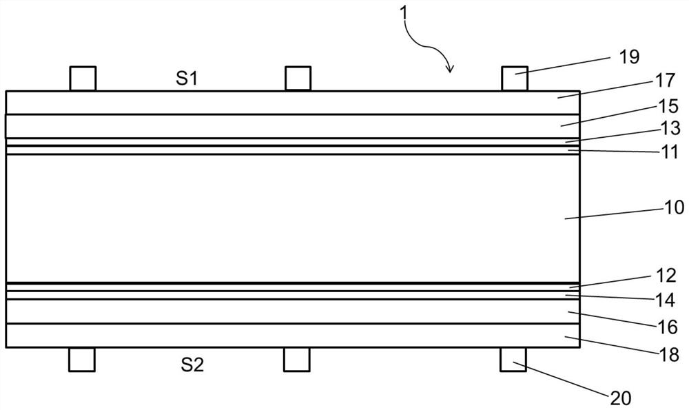
[0031] see figure 1 , which shows a schematic diagram of the composition and structure of the heterojunction solar cell of the present invention. like figure 1 As shown, the heterojunction solar cell 1 includes an N-type monocrystalline silicon wafer 10 . A first intrinsic amorphous silicon layer 11, a third intrinsic amorphous silicon layer 13, an N-type amorphous silicon layer 15, and...


PUM


Abstract

The invention provides a heterojunction solar cell and a manufacturing method thereof. The heterojunction solar cell comprises an N-type monocrystalline silicon wafer. A first intrinsic amorphous silicon layer, a third intrinsic amorphous silicon layer, an N-type amorphous silicon layer, a first transparent conductive film and a first electrode are sequentially formed on the front side of the N-type monocrystalline silicon wafer. A second intrinsic amorphous silicon layer, a fourth intrinsic amorphous silicon layer, a P-type amorphous silicon layer, a second transparent conducting film and a second electrode are sequentially formed on the back side of the N-type monocrystalline silicon wafer. The first intrinsic amorphous silicon layer and the second intrinsic amorphous silicon layer are formed through a first intrinsic PECVD process with the process gas being silane not doped with hydrogen. The third intrinsic amorphous silicon layer is formed through a second intrinsic PECVD process with process gases including carbon dioxide, hydrogen and silane, wherein the volume ratio of the carbon dioxide to the silane increases in a range of 0.1-0.6 as time increases. The fourth intrinsic amorphous silicon layer is formed through a third intrinsic PECVD (plasma enhanced chemical vapor deposition) process with process gases comprising hydrogen and silane. According to the invention, the cell conversion efficiency can be improved.

Description

technical field [0001] The invention relates to the field of solar cell manufacturing, in particular to a heterojunction solar cell and a manufacturing method thereof. Background technique [0002] Thin-film / crystalline silicon heterojunction solar cells (hereinafter referred to as heterojunction solar cells, also known as HIT or HJT or SHJ solar cells) belong to the third generation of high-efficiency solar cell technology, which combines the advantages of crystalline silicon and silicon thin films, and has With the characteristics of high conversion efficiency and low temperature coefficient, it will gradually replace PERC (Passivated Emitter and Rear Cell) cells and become the mainstream of photovoltaic cells. [0003] The core manufacturing process of heterojunction solar cells is the formation of various amorphous silicon films, including: the front and back sides of N-type crystalline silicon after surface texturing or texturing by plasma-enhanced chemical vapor deposi...

Claims


Application Information

Patent Timeline
IPC IPC(8): H01L31/20H01L21/02H01L31/0352H01L31/0376H01L31/0747C23C14/08C23C16/24C23C16/40C23C16/50C23C28/04
CPCH01L31/202H01L31/0747H01L31/03762H01L31/03529H01L21/02532H01L21/02592H01L21/0262C23C16/50C23C16/24C23C16/407C23C16/40C23C14/086C23C14/08C23C28/04Y02P70/50Y02E10/548
Inventor 马哲国王琳吴科俊汪训忠张效国钟潇
Owner 理想万里晖真空装备(泰兴)有限公司
Why Eureka
Try Eureka