Silicon-based heterojunction solar cell passivation layer early stage processing method

A solar cell and pre-treatment technology, applied in the direction of circuits, electrical components, sustainable manufacturing/processing, etc., can solve problems such as pollution, affecting the passivation effect of amorphous silicon passivation layer, increasing the density of defect states, etc., to achieve improved growth Quality, improvement of passivation effect, effect of reducing defect state density

Inactive Publication Date: 2015-11-25
IDEAL ENERGY (SHANGHAI) SUNFLOWER THIN FILM EQUIPMENT LTD
View PDF5 Cites 4 Cited by
  • Summary
  • Abstract
  • Description
  • Claims
  • Application Information

AI Technical Summary

Problems solved by technology

However, when the silicon wafer passes through the atmospheric environment, some other nanometer-sized structures will be formed on the surface of the silicon wafer, especially the top of the pyramid texture structure, which makes the smooth and round top become sharp, increasing the defect state density, Thereby affecting the passivation effect of preparing amorphous silicon passivation layer
[0007] In response to this problem, patent CN102779907A provides a method of introducing plasma etching during the wet processing of silicon wafers, the main purpose of which is to optimize the wet texturing process and improve surface light trapping through micro-etching treatment structure, but after the plasma etch is complete, the wafer goes back into the wet process and continues to be wet cleaned, so if the wafer is transferred to vacuum PECVD equipment to complete the passivation layer coating, Will face the same pollution problems as traditional production lines

Method used


Image

  • Silicon-based heterojunction solar cell passivation layer early stage processing method
  • Silicon-based heterojunction solar cell passivation layer early stage processing method

Examples


Embodiment Construction

[0029] In order to make the above objects, features and advantages of the present invention more comprehensible, specific implementations of the present invention will be described in detail below in conjunction with the accompanying drawings.

[0030] In the following description, many specific details are set forth in order to fully understand the present invention, but the present invention can also be implemented by other methods different from those described here, so the present invention is not limited by the specific embodiments disclosed below.

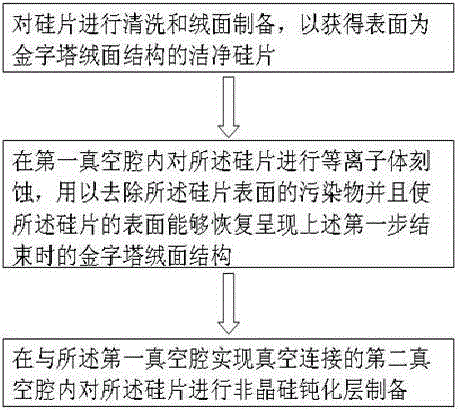
[0031] The invention provides a pre-treatment method for the passivation layer of a silicon-based heterojunction solar cell, the working process of which is as follows: figure 1 As shown, the method includes the following steps:

[0032] Step S1, cleaning the silicon wafer and preparing a suede surface to obtain a clean silicon wafer with a pyramid suede structure on the surface;

[0033] Step S2, performing plasma etching o...


PUM


Abstract

The invention provides a silicon-based heterojunction solar cell passivation layer early stage processing method. A plasma etching method is added after a silicon chip cleaning texturing step so as to make natural oxides or other impurities formed on the surface of a silicon chip removed. Meanwhile, micro etching is performed on the nanometer-sized tip of a pyramid textured structure of the silicon chip so as to make a smooth and round form thereof recovered. A passivation layer process is finally finished in a vacuum-maintained condition. Secondary pollution during the process is prevented. The passivation effects of an amorphous silicon passivation layer are thus improved. The passivation quality is guaranteed. The cell conversion efficiency is further improved.

Description

technical field [0001] The invention relates to the field of high-efficiency silicon-based heterojunction solar cells, in particular to a pre-treatment method for a passivation layer of a silicon-based heterojunction solar cell. technical background [0002] Silicon-based heterojunction solar cell is an emerging third-generation high-efficiency solar cell technology. It combines the advantages of the first-generation monocrystalline silicon and the second-generation silicon thin film, and has a series of advantages such as high conversion efficiency and low temperature coefficient. With great development potential and broad application prospects, it is expected to lead the development direction of the entire silicon-based solar cell. [0003] The preparation of the passivation layer is the most critical process step in the manufacturing process of silicon-based heterojunction solar cells. A high-quality passivation layer can effectively inhibit the recombination of carriers ...

Claims


Application Information

Patent Timeline
Patent Type & Authority Applications(China)
IPC IPC(8): H01L31/18
CPCY02P70/50
Inventor 陈金元吴科俊胡宏逵
Owner IDEAL ENERGY (SHANGHAI) SUNFLOWER THIN FILM EQUIPMENT LTD
Why Eureka
Try Eureka