Phase focusing image sensor and forming method thereof

An image sensor and phase focusing technology, which is applied in the direction of electric solid-state devices, semiconductor devices, electrical components, etc., can solve the problems of low focusing speed and precision, and poor performance of phase focusing image sensors, so as to increase the amount of incoming light and improve quantum Conversion efficiency, fast effect

Inactive Publication Date: 2019-03-08
HUAIAN IMAGING DEVICE MFGR CORP
View PDF3 Cites 9 Cited by
  • Summary
  • Abstract
  • Description
  • Claims
  • Application Information

AI Technical Summary

Problems solved by technology

[0004] However, since phase focusing needs to use pixels for phase detection, phase focusing has relatively high requirements on light intensity, and the focusing speed and accuracy are not high in dark and weak light environments, resulting in poor performance of phase focusing image sensors.

Method used


Image

  • Phase focusing image sensor and forming method thereof
  • Phase focusing image sensor and forming method thereof
  • Phase focusing image sensor and forming method thereof

Examples


Embodiment Construction

[0030] As mentioned in the background, the performance of prior art phase focusing image sensors is poor.

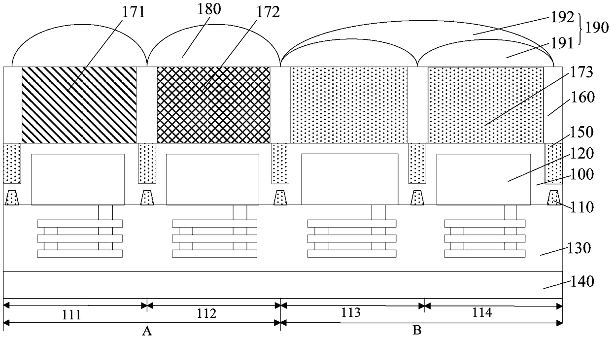
[0031] refer to figure 1 , figure 1 It is a structural schematic diagram of a phase focus image sensor, the phase focus image sensor includes a plurality of image capture units A and a plurality of phase focus units B, the image capture unit A and the phase focus unit include: a semiconductor substrate, the The semiconductor substrate has opposite first and second surfaces; a photosensitive structure 120 and an isolation structure 110 located in the semiconductor substrate 100, and the isolation structure 110 is located in the semiconductor substrate 100 between adjacent photosensitive structures 120; The interconnection structure 130 located on the first surface of the semiconductor substrate 100; the carrier 140 located on the surface of the interconnection structure 130; the light-receiving structure located on the second surface of the semiconductor substrate 100, t...


PUM


Abstract

The invention discloses a phase focusing image sensor and a forming method thereof. According to the method, a semiconductor substrate, a first photosensitive structure and a first filter layer are provided, wherein the semiconductor substrate comprises a phase focusing area and has a first surface and a second surface opposite to the first surface; the first photosensitive structure is located inthe phase focusing area of the semiconductor substrate; the first photosensitive structure comprises a first surface and a second surface opposite to the first surface; the first photosensitive structure comprises an absorption layer which is used for absorbing near infrared light; the first surface of the first photosensitive layer is exposed from the absorption layer; the first filter layer islocated on the second surface of the phase focusing area of the semiconductor substrate; and natural light passes through the first filter layer. The performance of the phase focusing image sensor isimproved.

Description

technical field [0001] The invention relates to the field of semiconductor manufacturing, in particular to a phase focus image sensor and a forming method thereof. Background technique [0002] An image sensor is a semiconductor device that converts light signals into electrical signals. At present, CMOS phase focusing image sensors have been widely used in digital still cameras, digital video cameras, medical imaging devices, and automotive imaging devices. [0003] At present, the focus methods used in mobile phone shooting are mainly contrast detection autofocus (contrast detection autofocus) and phase detect autofocus (PDAF for short). The principle of contrast focusing is to find the position of the lens with the maximum contrast according to the contrast change of the picture at the focal point, that is, the position of accurate focus. The principle of phase focusing is to reserve some pixels on the photosensitive element for phase detection, and determine the focus ...

Claims


Application Information

Patent Timeline
Patent Type & Authority Applications(China)
IPC IPC(8): H01L27/146
CPCH01L27/146H01L27/14601H01L27/14621H01L27/14627H01L27/14683H01L27/14685
Inventor 张东亮陈世杰黄晓橹
Owner HUAIAN IMAGING DEVICE MFGR CORP
Why Eureka
Try Eureka