

Semiconductor device and manufacturing method thereof
A semiconductor and conductive type technology, which is applied in semiconductor/solid-state device manufacturing, semiconductor devices, transistors, etc., can solve problems such as reducing on-resistance, and achieve the effect of improving latch-up damage tolerance
- Summary
- Abstract
- Description
- Claims
- Application Information
AI Technical Summary
Problems solved by technology
Method used
Image

Examples
Embodiment approach 1
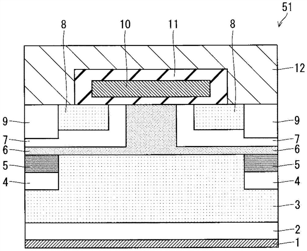
[0056] image 3 is a cross-sectional view showing the structure of the semiconductor device 51 according to the first embodiment. This semiconductor device 51 is a planar gate type SiC-IGBT using silicon carbide (SiC) as a semiconductor material. In addition, since silicon carbide is used as a semiconductor material, the semiconductor device 51 can operate stably even at high temperatures.
[0057] The semiconductor device 51 includes: a collector electrode 1; a collector region 2 of the first conductivity type; a drift region 3 of the second conductivity type; a buried region 4 of the first conductivity type; and a carrier trap region 5 of the second conductivity type. ; The carrier accumulation region 6 of the second conductivity type; The base region 7 of the first conductivity type; The emitter region 8 of the second conductivity type; The base contact region 9 of the first conductivity type; The gate electrode 10; an electrode oxide film 11; and an emitter electrode 12....
Embodiment approach 2
[0087] A semiconductor device according to Embodiment 2 of the present invention will be described as in Embodiment 1, taking a planar gate type SiC-IGBT using silicon carbide (SiC) as a semiconductor material as an example. Figure 11 It is a cross-sectional view showing the structure of the semiconductor device 52 according to the second embodiment. In the semiconductor device 52 according to the second embodiment, the image 3 In the semiconductor device 51 of , the carrier storage region 6 is not arranged under the base contact region 9 , and the carrier trap region 5 is connected to the base region 7 .
[0088] According to the semiconductor device 52 described in Embodiment 2, during the off operation of the SiC-IGBT, holes as minority carriers accumulated in the drift region 3 preferentially bypass the buried region 4 and reach the base contact region 9 . At this time, the holes directly reach the base region 7 without bypassing the carrier storage region 6 . Therefo...
Embodiment approach 3
[0090] A semiconductor device according to Embodiment 3 of the present invention will be described as in Embodiment 1, taking a planar gate type SiC-IGBT using silicon carbide (SiC) as a semiconductor material as an example. Figure 12 It is a cross-sectional view showing the structure of the semiconductor device 53 according to the third embodiment. In the semiconductor device 53 according to Embodiment 3, compared to the semiconductor devices 51 and 52 shown in Embodiments 1 and 2 above, the carrier trap region 5a has the first conductivity type instead of the second conductivity type. conductivity type. That is, the carrier trap region 5 a of the first conductivity type is disposed between the buried region 4 and the base region 7 . In addition, the impurity concentration of the first conductivity type in the carrier trapping region 5a is expected to be 1×10 15 cm -3 ~1×10 21 cm -3 In the range.
[0091] According to the semiconductor device 53 described in Embodiment...
PUM
 Abstract
Description
Claims
Application Information