LED COB packaging method and LED packaging module
A packaging method and module technology, applied in electrical components, electrical solid-state devices, circuits, etc., can solve the problems of difficult yield, cumbersome process, breakdown of pixel units, etc., to improve production efficiency and yield, and improve production efficiency. , The effect of preventing electrostatic breakdown
- Summary
- Abstract
- Description
- Claims
- Application Information
AI Technical Summary
Problems solved by technology
Method used
Image

Examples
Embodiment 1
[0064] image 3 A flow chart of the COB packaging method for LEDs provided in this embodiment, Figure 4 The state diagram of the glue pouring process of the COB packaging method of the LED provided in this embodiment is combined below image 3 with Figure 4 This embodiment will be specifically described.
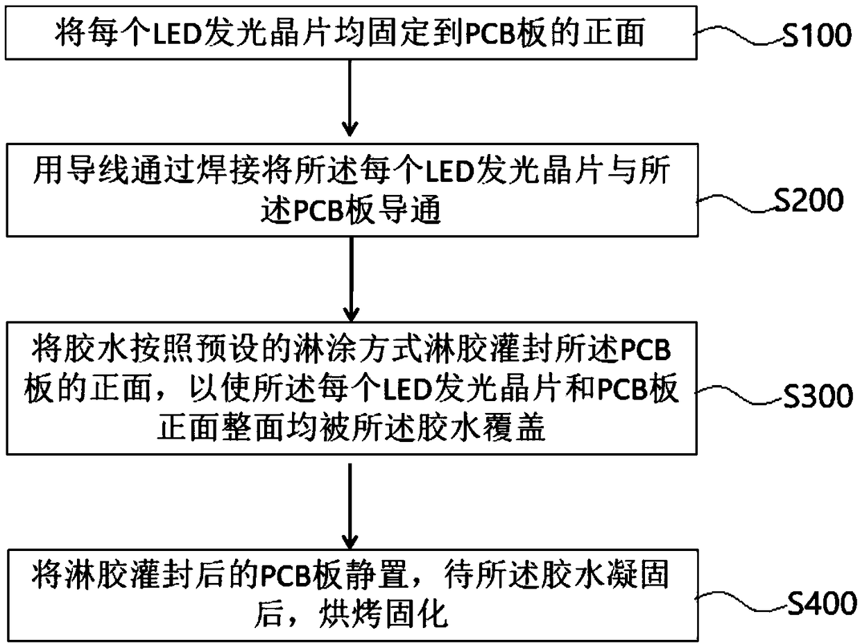
[0065] Such as image 3 As shown, the COB packaging method of LED provided in this embodiment at least includes the steps:
[0066] S100: Fix each LED light-emitting chip to the front of the PCB board;
[0067] S200: Connect each LED light-emitting chip to the PCB board by soldering with wires;
[0068] S300: Apply glue to the front of the PCB board according to the preset spraying method, so that each LED light-emitting chip and the entire front surface of the PCB board are continuously covered with glue;
[0069] S400: Leave the PCB board after glue pouring and potting to stand, and bake and solidify after the glue is solidified.
[0070] In this embodiment, the g...
Embodiment 2
[0097] The red light LED chip, the green light LED chip and the blue light LED chip in the LED light-emitting chip are respectively fixed on the PCB board through silver paste or insulating glue.
[0098] Connect the positive electrode of the red LED chip to the positive electrode pad on the PCB through a wire, and the negative electrode of the red LED chip is directly connected to the negative electrode pad on the PCB; connect the positive and negative electrodes of the green LED chip and the blue LED chip The poles are respectively connected to the positive and negative pads on the PCB through wires.
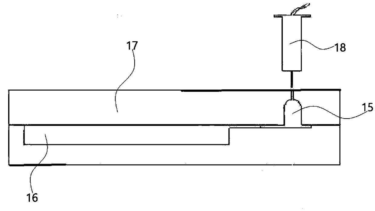
[0099] Multiple glue guns 600 are arranged at equal intervals on the first end 101 of the PCB, and the multiple glue guns 600 are placed above the PCB. There can be 2-5 glue guns, for example, 3 glue guns. Control the glue outlet of each glue gun to discharge glue continuously and evenly. Three glue guns spray glue on the PCB board at the same time, and spray glue continuousl...
Embodiment 3
[0103] Figure 5 A schematic diagram of the longitudinal section structure of the LED packaging module provided in this embodiment, Image 6 The top view of the LED packaging module provided by this embodiment, Figure 7 A partial schematic diagram of the LED packaging module provided for this embodiment, combined below Figure 5-7 This embodiment will be specifically described.
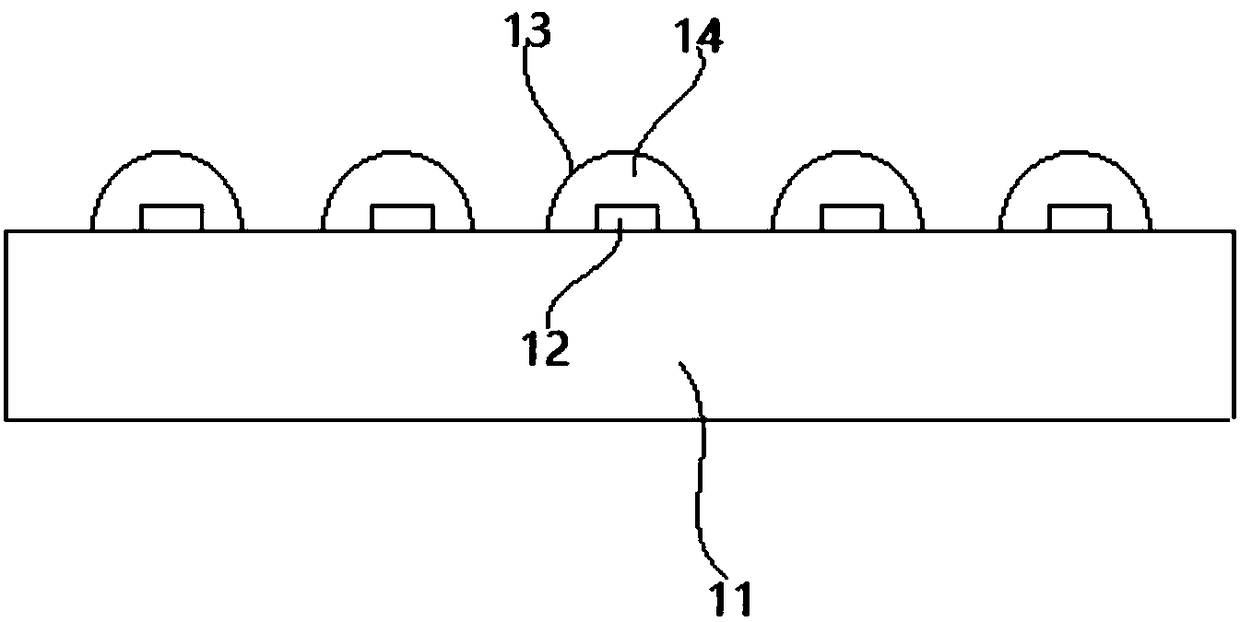
[0104] Such as Figure 5 As shown, the LED packaging module prepared according to the LED COB packaging method described in the above embodiments includes: a PCB board 100, a plurality of LED light-emitting chips 200 and a colloidal layer 300;
[0105] A plurality of LED light-emitting chips 200 are fixed on the front of the PCB board 100, and each LED light-emitting chip 200 is electrically connected to the PCB board 100 through a wire 400;
[0106] The colloidal layer 300 is covered on the front of the PCB 100 by pouring glue, so that each LED light-emitting chip 200 and the entire front of the P...
PUM
| Property | Measurement | Unit |
|---|---|---|
| Width | aaaaa | aaaaa |
| Length | aaaaa | aaaaa |
Abstract
Description
Claims
Application Information