Supercharge Your Innovation With Domain-Expert AI Agents!

A method for flattening gan deep trenches for leds

A manufacturing method and planarization technology, which can be applied to semiconductor devices, electrical components, circuits, etc., can solve the problem of inability to achieve planarization of GaN deep grooves, and achieve the effects of high yield, easy manufacturing process, and consistent thickness

Active Publication Date: 2020-04-28
JIANGSU XGL OPTOELECTRONICS
View PDF3 Cites 0 Cited by
  • Summary
  • Abstract
  • Description
  • Claims
  • Application Information

AI Technical Summary

Problems solved by technology

However, as mentioned above, because the stability of PSS is far superior to that of GaN-based epitaxial layers, the current etching technology cannot achieve GaN deep trench planarization.

Method used


Image

  • A method for flattening gan deep trenches for leds
  • A method for flattening gan deep trenches for leds
  • A method for flattening gan deep trenches for leds

Examples


Embodiment 1

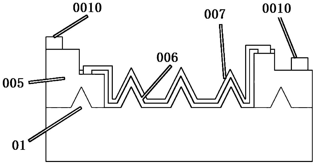
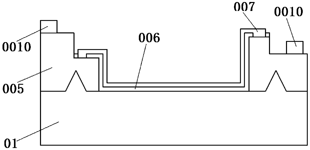
[0038] Embodiment 1: A method for making GaN deep trench planarization for LEDs, comprising the following steps:

[0039] Step 1. Select the sapphire flat substrate 001, and deposit a layer of insulating layer 002 on the sapphire flat substrate 001;

[0040] In this embodiment, the insulating layer 002 includes SiO 2 ;

[0041] Step 2. Form a patterned first mask window 003 on the insulating layer 002 through a photolithography process;

[0042] Step 3. Etching the insulating layer 002 under the cover of the first mask window 003 through an etching process to obtain a tapered insulating layer 004, and removing the first mask window 003;

[0043] The etching process adopts ICP dry etching. By adjusting the radio frequency power and the power of the upper and lower electrodes of the etching equipment, the lateral etching of the insulating layer 002 is increased, so that the insulating layer 002 is etched into a tapered insulating layer 004; due to the flat sapphire substrate ...


PUM

PropertyMeasurementUnit
widthaaaaaaaaaa
heightaaaaaaaaaa

Abstract

The invention, which belongs to the technical field of LED chips, provides a making method for GaN deep trench planarization of an LED. The method comprises the following steps: making an insulating layer; making a tapered insulating layer; growing an epitaxial layer; etching the epitaxial layer; etching a GaN deep trench; making an insulating dielectric layer; and making a conductive metal layer.According to the invention, the patterned insulating layer is introduced on the sapphire flat substrate; and since the patterned insulating layer is easy to etch, planarization of the GaN deep trenchcan be realized by using a dry etching process when the GaN deep trench is etched. Therefore, the brightness of the LED is improved; the uniformity of the conventional process film layer is enhancedsubstantially; and the reliability of the device is improved.

Description

technical field [0001] The invention relates to a method for manufacturing a GaN deep groove planarization process, in particular to a method for manufacturing a GaN deep groove planarization process for LEDs, and belongs to the technical field of LED chips. Background technique [0002] Patterned Sapphire Substrates (PSS) is the preferred substrate material for gallium nitride (GaN) material epitaxy, and the epitaxy technology based on PSS is the mainstream technology used in the LED industry. PSS is to produce periodic sapphire pattern structure on sapphire flat sheet through photolithography and dry etching technology. A single pattern is a cone with a bottom width of 2.5-3.0 microns and a height of 1.6-1.8 microns. Compared with sapphire flat film, PSS can improve the LED light efficiency index by about 30%. As a key technology for LED industry applications, it will continue to become the mainstream. [0003] Although PSS graphics have the advantage of improving LED bri...

Claims


Application Information

Patent Timeline
Patent Type & Authority Patents(China)
IPC IPC(8): H01L33/22H01L33/44H01L33/00
CPCH01L33/0066H01L33/0075H01L33/22H01L33/44H01L2933/0025
Inventor 华斌黄慧诗闫晓密
Owner JIANGSU XGL OPTOELECTRONICS
Features
  • R&D
  • Intellectual Property
  • Life Sciences
  • Materials
  • Tech Scout
  • Unparalleled Data Quality
  • Higher Quality Content
  • 60% Fewer Hallucinations
Learn More