Method for manufacturing MOS transistor with germanium silicon source and drain

A MOS transistor, silicon germanium source-drain technology, applied in semiconductor/solid-state device manufacturing, electrical components, circuits, etc., can solve problems such as adverse effects on device performance, deformation of groove morphology, and loss of oxide layer.

Active Publication Date: 2019-03-29
SHANGHAI HUALI INTEGRATED CIRCUTE MFG CO LTD
View PDF6 Cites 2 Cited by
  • Summary
  • Abstract
  • Description
  • Claims
  • Application Information

AI Technical Summary

Problems solved by technology

[0003] In the existing methods, for the pollutants such as polymer or byproduct on the surface of high pollutants, the existing methods are to use acid tank (wet bench tool) or single wafer cleaning machine (single wafer) to add DHF to clean, but with As the line width shrinks, the overall loss (loss) of the silicon substrate caused by cleaning must also be taken into account. The loss caused by DHF is mainly the loss of the oxide layer, so it is extremely important to control the number of seconds of DHF clean

Method used


Image

  • Method for manufacturing MOS transistor with germanium silicon source and drain
  • Method for manufacturing MOS transistor with germanium silicon source and drain
  • Method for manufacturing MOS transistor with germanium silicon source and drain

Examples


Embodiment Construction

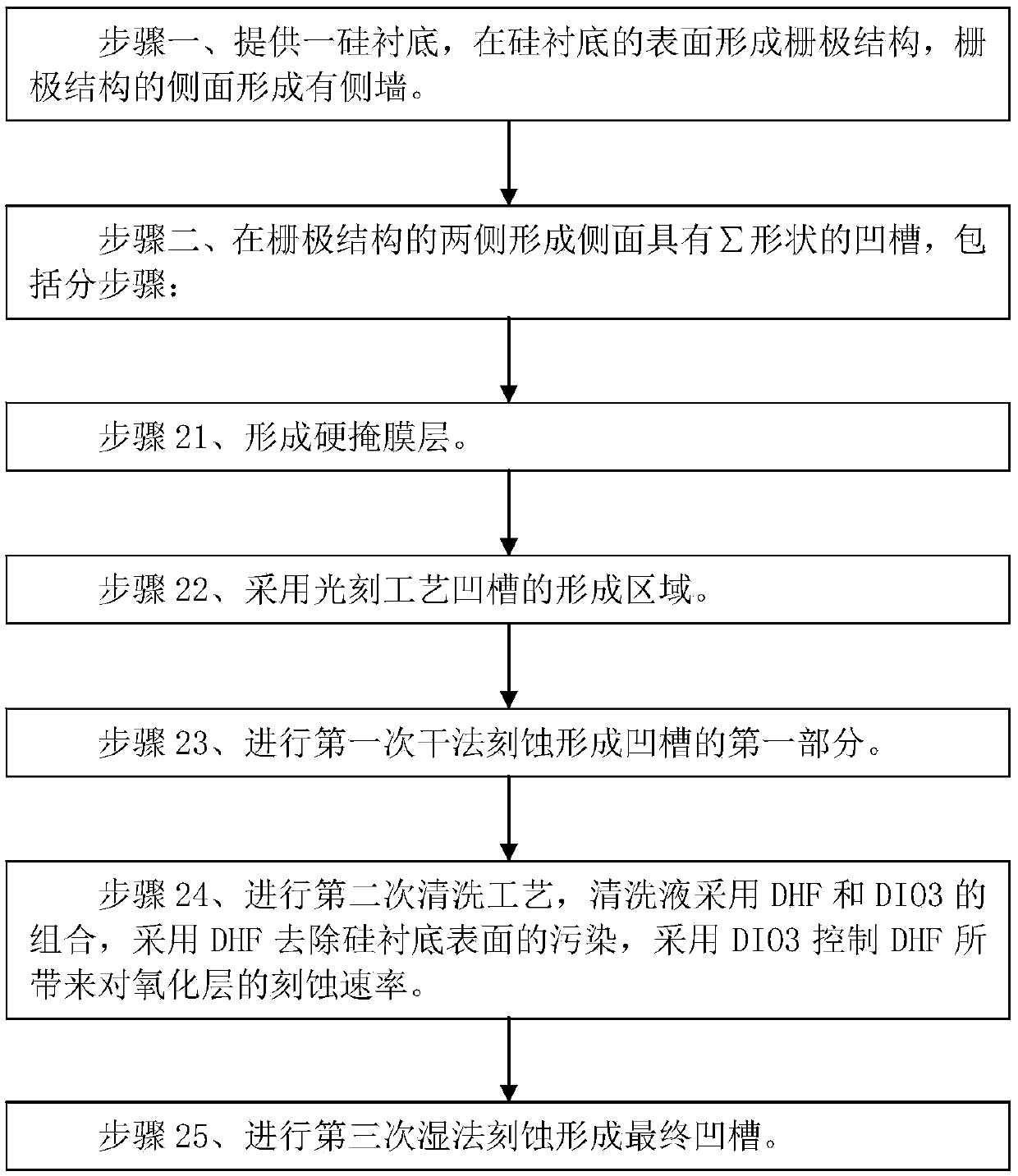
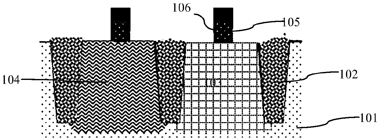
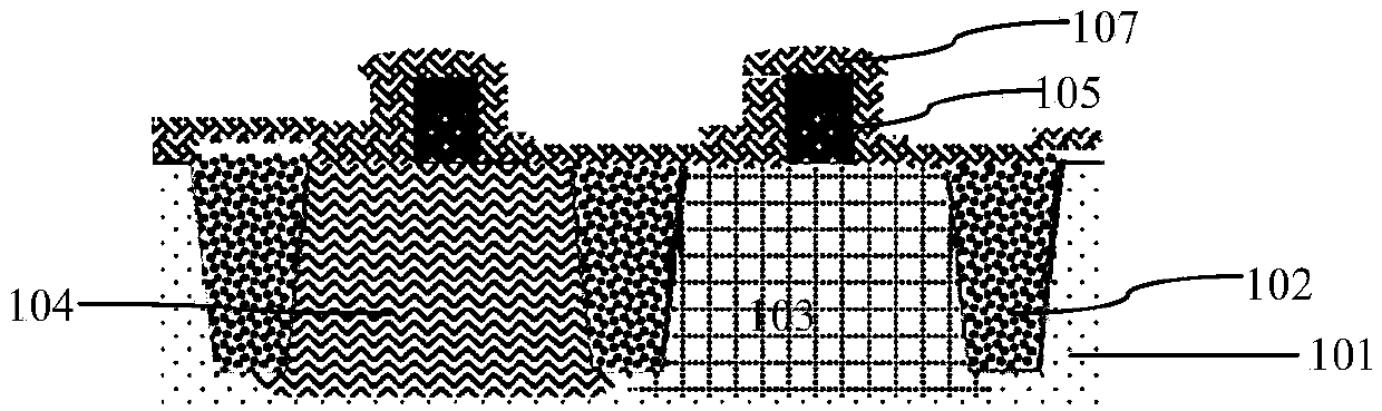
[0036] like figure 1 Shown is the flow chart of the method of the embodiment of the present invention; Figure 2A to Figure 2D As shown, it is a device structure diagram in each step of the method of the embodiment of the present invention. The manufacturing method of the MOS transistor with silicon germanium source and drain in the embodiment of the present invention includes the following steps:

[0037] Step 1, such as Figure 2A As shown, a silicon substrate 101 is provided, a gate structure 105 is formed on the surface of the silicon substrate 101, side walls 106 are formed on the side of the gate structure 105, and the side walls 106 also extend to the gate The surface of the pole structure 105.

[0038] A shallow trench field oxygen is formed on the surface of the silicon substrate 101, an active region is isolated by the shallow trench field oxygen, and a MOS transistor is formed in the active region.

[0039] The MOS transistor with silicon germanium source and dra...


PUM


Abstract

The invention discloses a method for manufacturing an MOS transistor with a germanium silicon source and drain. The method comprises steps that S1, a silicon substrate is provided, a gate structure isformed on a surface of the silicon substrate, and a side wall is formed on a side surface of the gate structure; and S2, a groove having the meandering shape is formed on two sides of the gate structure, including sub steps of S21, a hard mask layer is formed; S22, a formation region of the groove of the photolithography process is employed; S23, first dry etching is performed to form a first portion of the groove; S24, second cleaning process is performed, the cleaning solution adopts the combination of DHF and DIO3, the DHF is employed to remove contamination on the surface of the silicon substrate, the DIO3 is employed to control the etching rate of the oxide layer brought by the DHF, and S25, third wet etching is performed to form a final groove. The method is advantaged in that control of the cleaning process after the groove is dry can be realized, and loss of an oxide layer can be reduced or avoided while the contamination on the surface of the silicon substrate can be sufficiently removed.

Description

technical field [0001] The invention relates to a method for manufacturing a semiconductor integrated circuit, in particular to a method for manufacturing a MOS transistor with silicon germanium source and drain. Background technique [0002] The source and drain regions of MOS transistors, especially PMOS transistors, often need to form an embedded silicon germanium epitaxial layer. The embedded silicon germanium epitaxial layer can modulate the stress of the channel region of the PMOS transistor, which is conducive to improving the carrier mobility of the PMOS. Therefore, the electrical performance of the PMOS tube is improved. However, the embedded silicon germanium epitaxial layer is introduced by first forming a groove in the silicon substrate, the groove usually has a Σ shape, and then filling the epitaxial layer in the groove to realize the embedding of the epitaxial layer into the silicon substrate. The etching process of the groove needs to use a hard mask layer, a...

Claims


Application Information

Patent Timeline
IPC IPC(8): H01L21/02H01L21/8234
CPCH01L21/02057H01L21/823418
Inventor 刘厥扬
Owner SHANGHAI HUALI INTEGRATED CIRCUTE MFG CO LTD
Why Eureka
Try Eureka