P-type crystalline silicon solar cell and preparation method thereof

A technology of crystalline silicon solar cells and p-type silicon, applied in the field of solar cells, can solve problems such as limiting battery open circuit voltage and other performance parameters, increasing recombination and loss, etc., achieve high open circuit voltage and photoelectric conversion efficiency, reduce recombination and loss, The effect of increasing concentration

Inactive Publication Date: 2019-04-02
SHANGHAI ADVANCED RES INST CHINESE ACADEMY OF SCI
View PDF5 Cites 0 Cited by
  • Summary
  • Abstract
  • Description
  • Claims
  • Application Information

AI Technical Summary

Problems solved by technology

However, in the existing PERC cell structure, the photogenerated carriers away from the local aluminum back field region need to travel a certain distance laterally to be collected by the aluminum bac

Method used


Image

  • P-type crystalline silicon solar cell and preparation method thereof
  • P-type crystalline silicon solar cell and preparation method thereof
  • P-type crystalline silicon solar cell and preparation method thereof

Examples


Embodiment 1

[0076] Such as Figure 1 to Figure 7 As shown, this embodiment provides a method for preparing a p-type crystalline silicon solar cell, comprising steps:

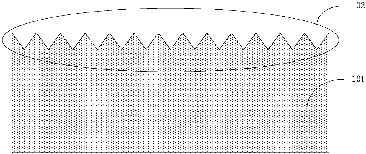
[0077] Such as figure 1 As shown, perform step 1) to provide a p-type crystalline silicon substrate 101, and use texturing treatment to form a textured light-trapping structure 102 on the front surface of the p-type crystalline silicon substrate 101.

[0078] As an example, the thickness of the p-type crystalline silicon substrate 101 is between 40-200 μm, the resistivity of the p-type crystalline silicon substrate 101 is between 0.5-3 Ω·cm, and the p-type crystalline silicon substrate 101 may be a single crystal Silicon can also be polysilicon.

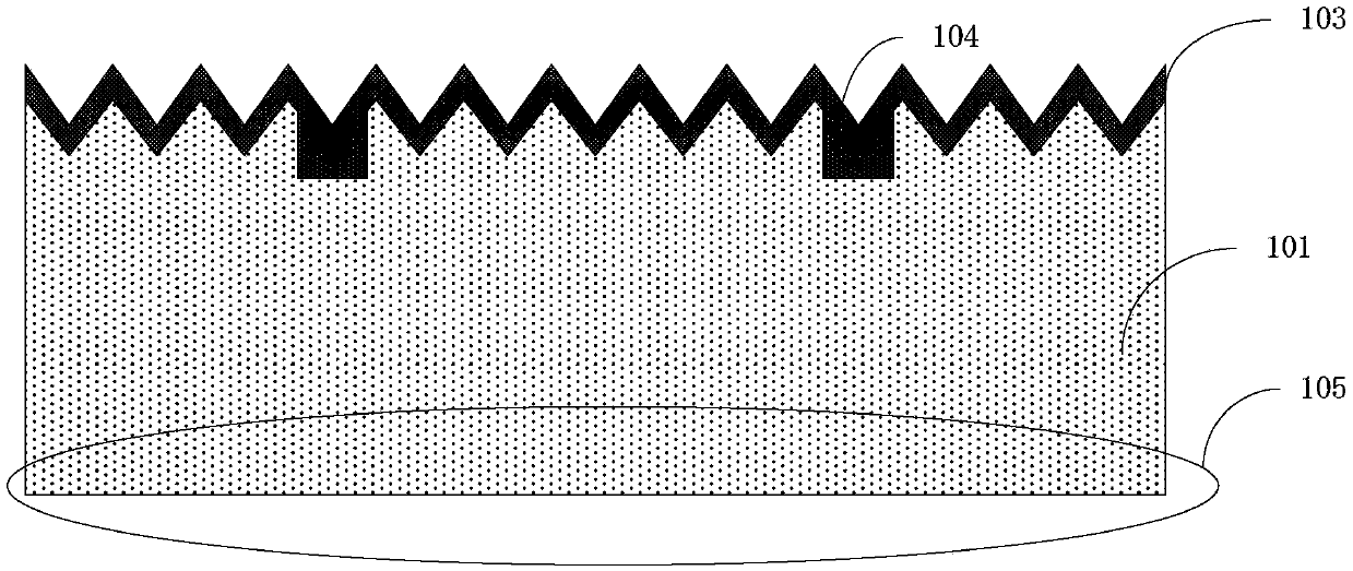
[0079] Such as figure 2 As shown, proceed to step 2) form an n-type doped layer 103 on the front surface of the p-type crystalline silicon substrate 101 by using phosphorus diffusion process, and the n-type doped layer 103 forms a pn junction with the p-type crystalline silico...

Embodiment 2

[0128] Such as Figure 9 As shown, the difference between this embodiment and Embodiment 1 is only that: in this embodiment, no heavily doped n-type layer 104 is provided.

[0129] Table 1

[0130]

[0131]Table 1 is the battery performance parameters of Example 1 and Example 2.

[0132] In summary, the present invention provides a p-type crystalline silicon solar cell and its preparation method, which have the following effects:

[0133] A heavily doped n-type layer 104 is formed on the front surface of the p-type crystalline silicon substrate 101, and the heavily doped n-type layer 104 has a certain promoting effect on the overall performance of the solar cell.

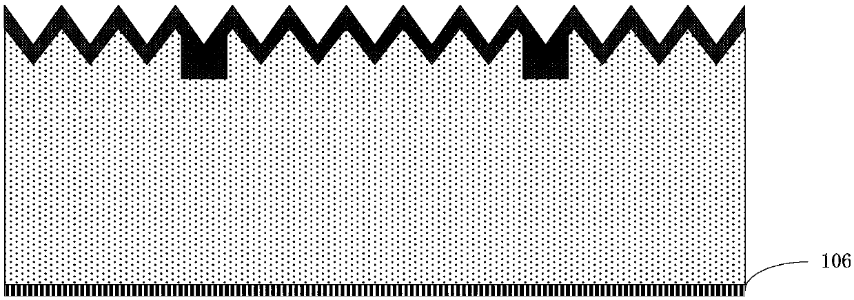
[0134] The shape 105 of the back surface of the p-type crystalline silicon substrate 101 includes a plane and textured light-trapping structure. When light is incident from the front surface of the p-type crystalline silicon substrate 101, the structure with a planar back surface has a relatively large short-ci...


PUM

PropertyMeasurementUnit
Thicknessaaaaaaaaaa
Thicknessaaaaaaaaaa
Thicknessaaaaaaaaaa

Abstract

The invention provides a p-type crystalline silicon solar cell and a preparation method thereof. The p-type crystalline silicon solar cell is characterized in that the back surface of a p-type crystalline silicon substrate is provided with a first oxide layer, a doped p-type silicon-based thin film layer, a second oxide layer and a silicon-based thin film layer which are sequentially stacked so asto form a laminated structure; a back contact window is formed in the laminated structure, and a metal grid line electrode is formed in the back contact window, wherein an ohmic contact is formed between the metal grid line electrode and one or both of the p-type crystalline silicon substrate and the doped p-type silicon-based thin film layer. According to the method, the hole concentration and the transverse transmission performance of the surface of the p-type crystalline silicon substrate can be improved, and recombination and loss of carriers are reduced; and compared with an existing PERC battery (Passivated Emitter and Rear Cell), a passivation emitter back battery), higher open-circuit voltage and photoelectric conversion efficiency can be obtained.

Description

technical field [0001] The invention belongs to the field of solar cells, in particular to a p-type crystalline silicon solar cell and a preparation method. Background technique [0002] PERC (Passivated Emitter and Rear Cell) p-type crystalline silicon solar cells can increase the photoelectric conversion efficiency of traditional full-area contact aluminum back field cells by more than 1%, and the manufacturing process is compatible with existing production lines. The main feature of PERC cells is that by using Al on the back of p-type silicon 2 o 3 The structural design of / SiNx laminated film and local aluminum back field reduces carrier recombination on the back of traditional full-area contact aluminum back field cells and parasitic light absorption of metal electrodes. However, in the existing PERC cell structure, the photogenerated carriers away from the local aluminum back field region need to travel a certain distance laterally to be collected by the aluminum bac...

Claims


Application Information

Patent Timeline
IPC IPC(8): H01L31/0224H01L31/0236H01L31/068H01L31/18
CPCH01L31/022441H01L31/02363H01L31/0684H01L31/1804Y02E10/547Y02P70/50
Inventor 鲁林峰王鹏陈小源方小红李东栋杨立友李高非王继磊
Owner SHANGHAI ADVANCED RES INST CHINESE ACADEMY OF SCI
Why Eureka
Try Eureka