Lamb wave resonator and preparation method thereof

A Lamb wave resonator and resonator technology, applied in impedance networks, electrical components, microstructure technology, etc., can solve the problems of poor crystal quality and the performance of Lamb wave resonators are smaller than expected, and achieve the effect of improving device performance.

Active Publication Date: 2019-04-02
INST OF SEMICONDUCTORS - CHINESE ACAD OF SCI
View PDF7 Cites 8 Cited by
  • Summary
  • Abstract
  • Description
  • Claims
  • Application Information

AI Technical Summary

Problems solved by technology

However, all the reported piezoelectric films of AlN-based Lamb wave resonators are polycrystalline AlN films based on magnetron sputtering technology, and the X-ray diffraction (XRD) rocking curve of AlN films prepared by this method is half of The height and width are between 2-5°, so the crystal quality is poor, resulting in the performance of the developed Lamb wave resonator being far less than expected

Method used


Image

  • Lamb wave resonator and preparation method thereof
  • Lamb wave resonator and preparation method thereof
  • Lamb wave resonator and preparation method thereof

Examples


preparation example Construction

[0033]In addition, the present invention proposes a method for preparing a Lamb wave resonator, which includes the following steps: Step 1, growing a single crystal nitride thin film layer on a base material at high temperature, and successively growing a single crystal nitride thin film layer on the upper surface of the single crystal nitride thin film layer. Form a bottom electrode layer, a dielectric sacrificial layer and a base support layer; step 2, remove the base material, and prepare interdigitated electrodes in the central area of ​​the lower surface of the single crystal nitride film layer; step 3, solder the devices in step 2 by solder On the substrate layer, and form a gap between the interdigital electrodes and the substrate layer; step 4, corrode the dielectric sacrificial layer to remove the dielectric sacrificial layer and the base support layer, and complete the preparation of the Lamb wave resonator.

[0034] Due to the combination of welding and corrosion pro...

Embodiment

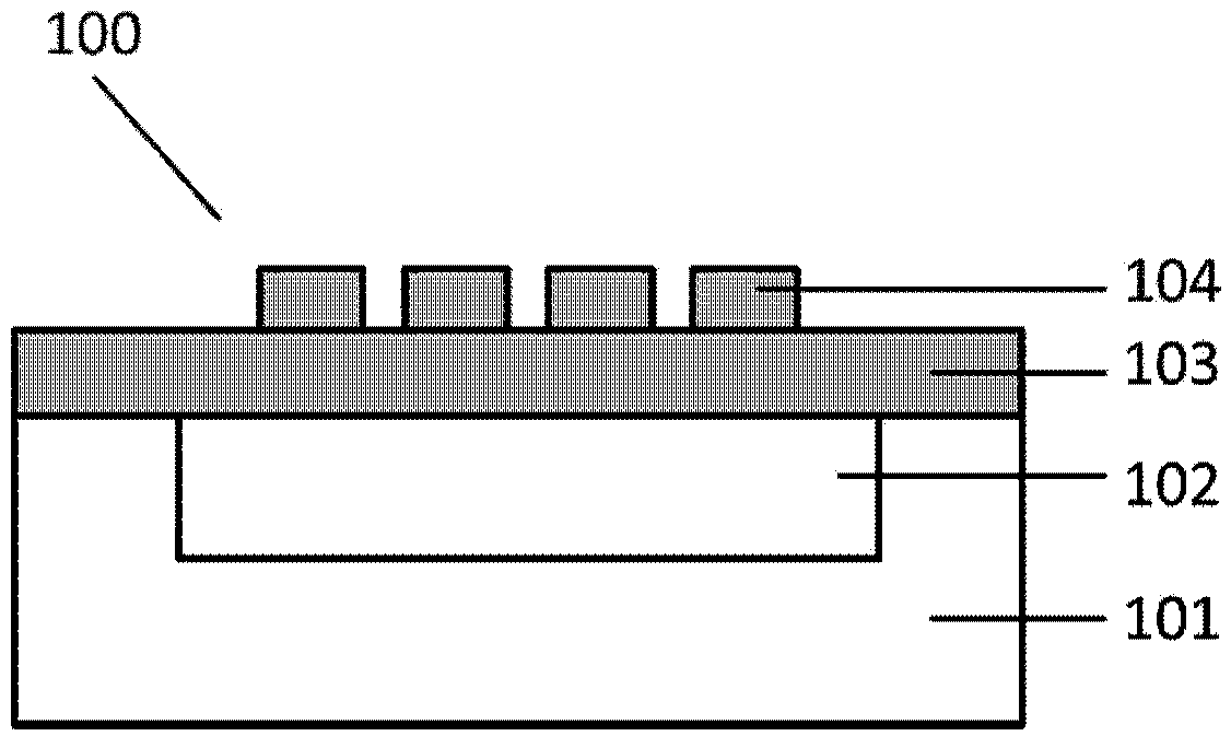
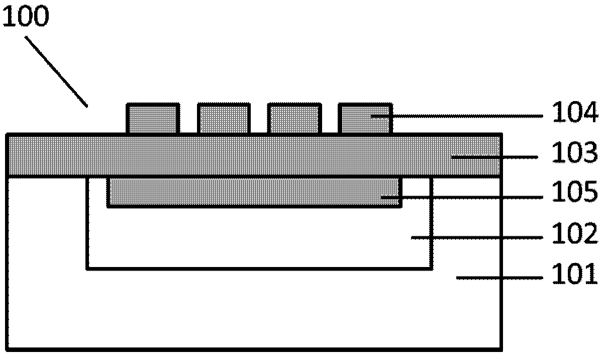
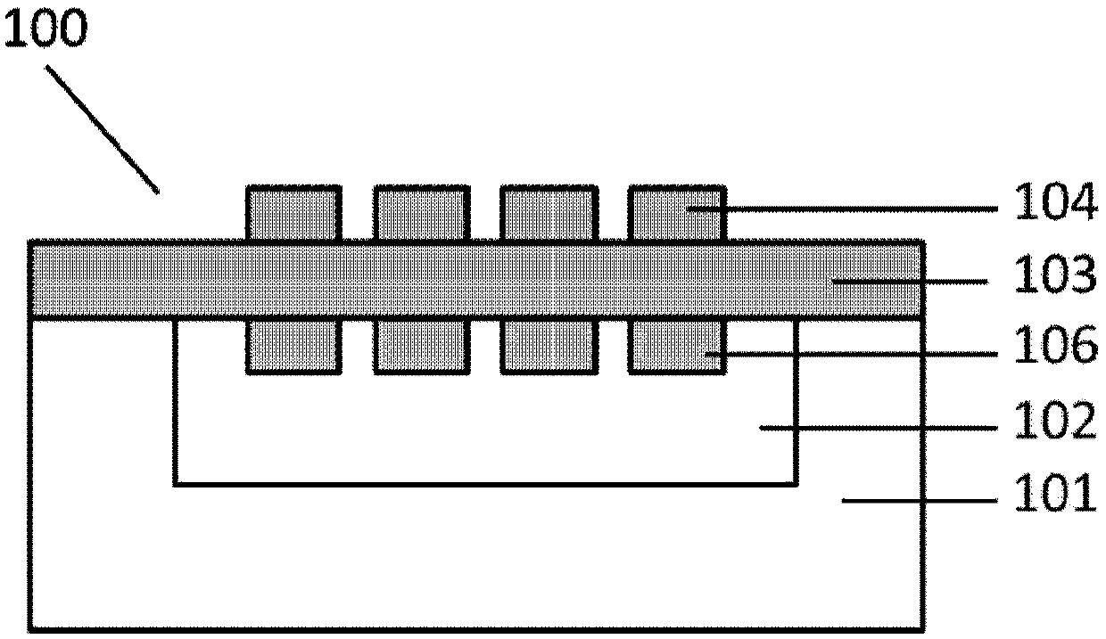
[0044] Such as Figure 4 As shown, the present embodiment proposes a Lamb wave resonator 200, including a substrate layer 210 and a resonator structure 220. The resonator structure includes a bottom electrode layer 221, a single crystal nitride thin film layer 222 and interdigitated fingers from bottom to top. An electrode 223, wherein: the interdigitated electrode 223 is located in the central region of the single crystal nitride thin film layer 222; the resonator structure 220 is placed upside down on the upper surface of the substrate layer 210, and a metal layer 230 is arranged between the resonator structure 220 and the substrate layer 210, There is a gap between the interdigital electrodes 223 and the substrate layer 210 .

[0045] This embodiment also proposes a Figure 4 The preparation method of the shown Lamb wave resonator 200 is as follows in conjunction with the attached Figure 5(a) ~ Figure 5(g) , the preparation method is described in detail, specifically com...


PUM


Abstract

The invention relates to a Lamb wave resonator and a preparation method thereof. The Lamb wave resonator comprises a substrate layer and a resonator structure, wherein the resonator structure includesa bottom electrode layer, a monocrystalline nitride film layer and an interdigital electrode from the bottom up, and the interdigital electrode is located in a central region of the monocrystalline nitride film layer; the resonator structure is arranged on the upper surface of the substrate layer in an inverted manner, a metal layer is arranged between the resonator structure and the substrate layer so as to enable the interdigital electrode and the substrate layer to have a gap therebetween. The invention combines welding and corrosion technologies, firstly the monocrystalline nitride film layer grows at a high temperature on a substrate material, and then the bottom electrode layer is formed on the monocrystalline nitride film layer, thereby avoiding the problems of surface roughening and easy reaction with an ammonia gas of the bottom electrode layer due to the formation of the film layer at a high temperature on the bottom electrode layer, and thus laying a foundation for the development of a monocrystalline nitride Lamb wave resonator.

Description

technical field [0001] The invention belongs to the research field of radio frequency MEMS devices, and more specifically relates to a Lamb wave resonator and a preparation method thereof. Background technique [0002] RF MEMS (Micro-Electro-Mechanical Systems) resonators based on the piezoelectric effect play an important role in the field of communication and are widely used. For example, quartz crystal resonators are ideal clock sources for radio frequency oscillators due to their extremely high quality factors; surface acoustic wave (SAW) resonators and filters are widely used in mobile communication filters due to their simple preparation process and excellent performance. The field has dominated for a long time; bulk acoustic wave (BAW) resonators and filters are gradually replacing SAW filters in the field of mobile communications due to their excellent performance, although the manufacturing process is more complicated than that of SAW filters. With more and more mo...

Claims


Application Information

Patent Timeline
Patent Type & Authority Applications(China)
IPC IPC(8): H03H3/02H03H9/02H03H9/24
CPCB81B2201/0271H03H3/02H03H9/02338H03H9/2405H03H2003/027H03H2009/02299
Inventor 艾玉杰张韵杨帅孙莉莉程哲张连贾丽芳王军喜李晋闽
Owner INST OF SEMICONDUCTORS - CHINESE ACAD OF SCI
Why Eureka
Try Eureka