Multilayer substrate cleaning method, substrate bonding method, and bonded wafer manufacturing method

Active Publication Date: 2007-02-01
SHIN-ETSU HANDOTAI CO LTD
View PDF6 Cites 16 Cited by
  • Summary
  • Abstract
  • Description
  • Claims
  • Application Information

AI Technical Summary

Benefits of technology

[0050] If a temperature when a Si layer of the surface of the delaminated layer is made to be a thermal oxide film by subjecting the surface to thermal oxidation is 1000° C. or less, generation of defects such as OSF (Oxidation induced Stacking Fault) can be prevented when damage by the ion implantation which remains in the Si layer of a surface of the delaminated layer is introduced into the thermal oxide film to be formed.
[0051] According to the present invention, if a protective film is formed on a surface of a SiGe layer and then the protective film is cleaned with a first cleaning liquid so that the protective film remains, the SiGe layer is protected during the cleaning and roughening of the surface can be prevented. In addition, because the protective film is slightly etched and removed with the first cleaning liquid, cleaning effect can be high and bonding force of the bonded plane can be prevented from lowering.
[0052] Moreover, if the multilayer substrate cleaned with the first cleaning liquid is cleaned with a second cleaning liquid which is capable of etching the protective film and which has a smaller etching rate for the protective film than the first cleaning liquid so that the protective film is removed and that the SiGe layer is exposed, the SiGe layer is etched with the second cleaning liquid having a small etching rate so that roughening of the surface is not caused. Therefore, roughening of a surface of the SiGe layer to be a bonded plane is prevented and at the same time the cleaning effect can be very high, thereby bonding force of the bonded plane can be prevented from lowering.
[0053] Furthermore, if a surface of the SiGe layer or the protective film cleaned by using the cleaning method as described above and a surf

Problems solved by technology

As described above, in the case that a bonded wafer is produced by using an ion implantation delamination method, there has been a problem that contamination such as organic matter and metal impurities or roughening of a surface is caused on a surface such as a Si1-XGeX layer, a Si layer, and an insulator layer which are implanted surfaces when ions are implanted.
Such voids or blisters degrade process yield of producing bonded wafers.
Such lowering of bonding force of the bonded plane causes

Method used


Image

  • Multilayer substrate cleaning method, substrate bonding method, and bonded wafer manufacturing method
  • Multilayer substrate cleaning method, substrate bonding method, and bonded wafer manufacturing method
  • Multilayer substrate cleaning method, substrate bonding method, and bonded wafer manufacturing method

Examples


examples 1 and 2

, COMPARATIVE EXAMPLES 1-3

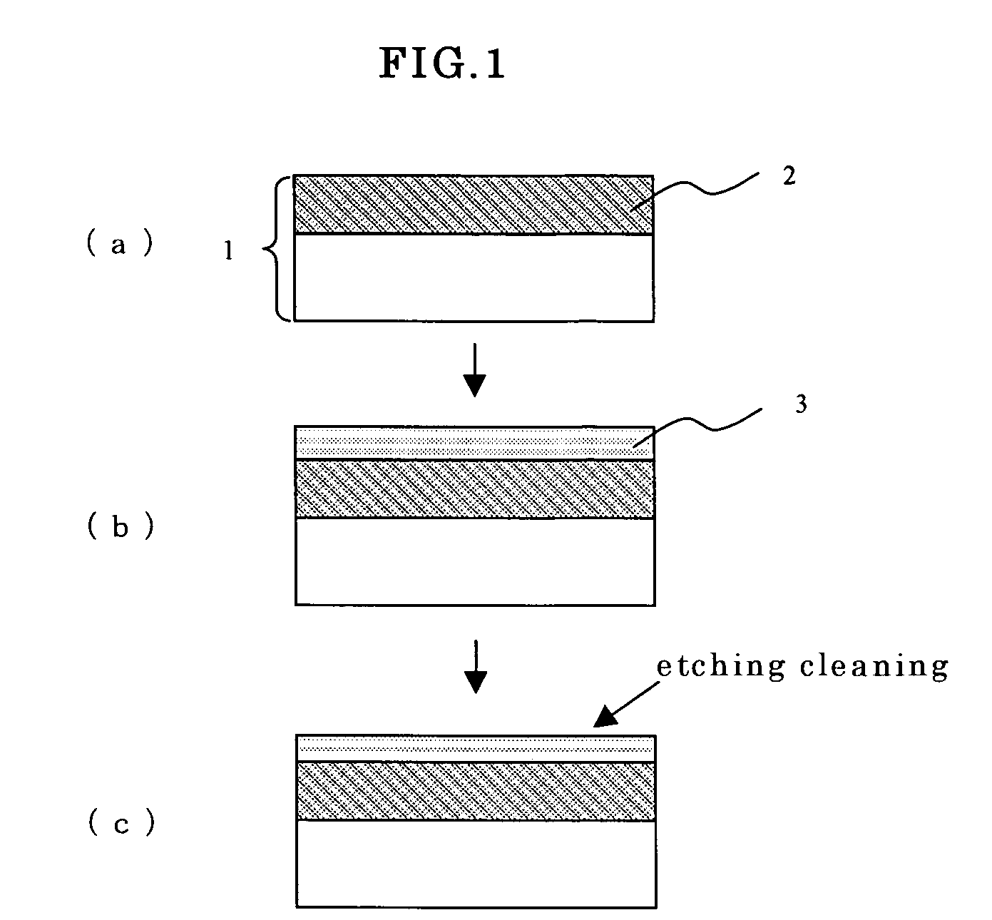
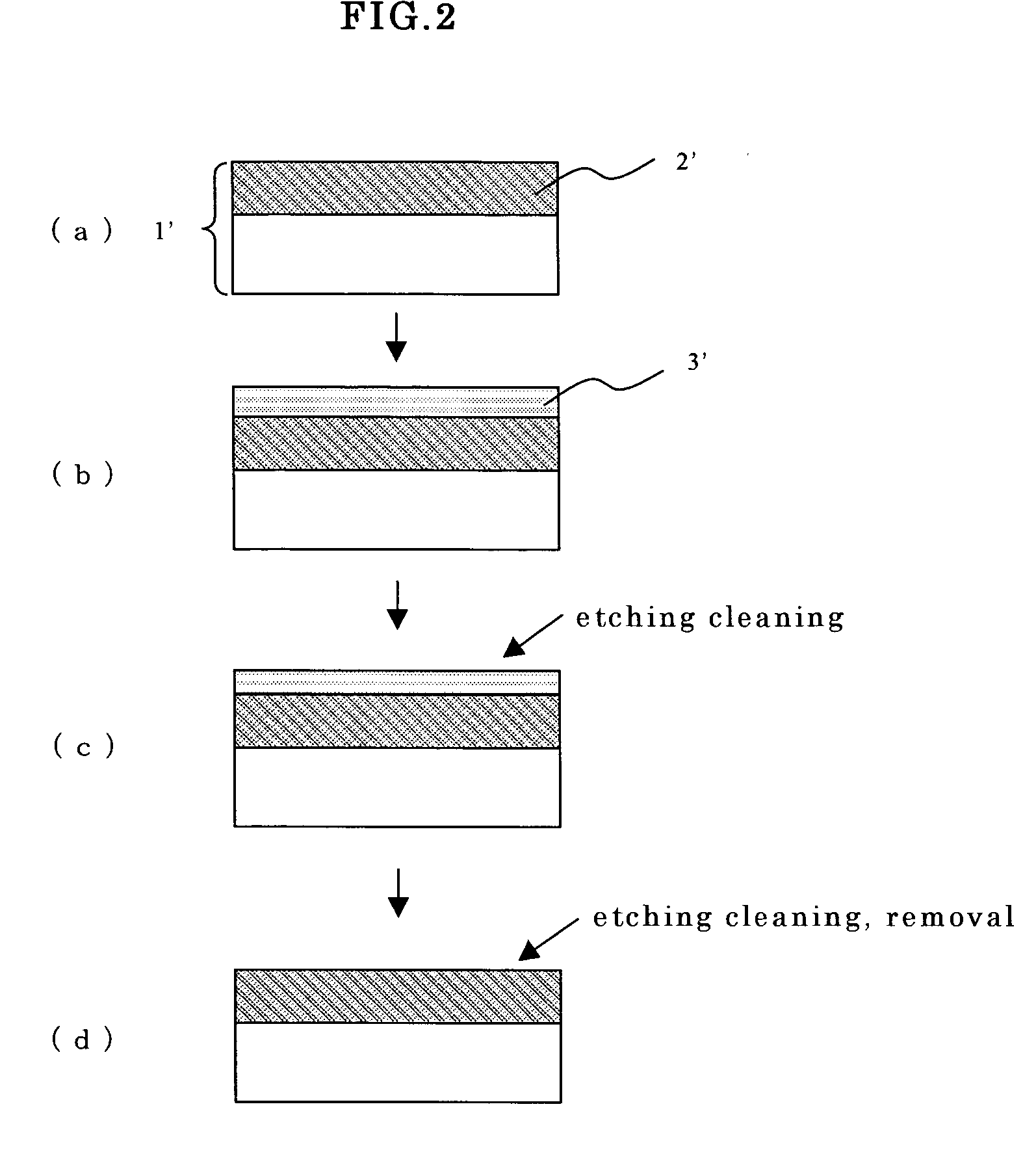
[0108] A total of 4 kinds of sample wafers were prepared: on a surface (a mirror-polished surface) of a silicon single crystal wafer having a diameter of 200 mm, a SiGe layer with a Ge concentration of 5% or 15% is deposited only by 50 nm by epitaxial method to be an uppermost surface layer as shown in Table 1 as described below (Comparative Examples 1 and 2), and as a protective film, a protective silicon layer is further deposited thereon only by 20 nm by epitaxial method to be an uppermost surface layer (Examples 1 and 2). Moreover, for a reference, a general mirror-polished silicon single crystal wafer without the above-described epitaxial layer being formed (Comparative Example 3) was prepared.

[0109] The surface of each uppermost surface layer of the five kinds of the sample wafers and silicon single crystal base wafers that were separately prepared (having a thermal oxide film with a thickness of 400 nm) were subjected to SC-1 cleaning in conditions ...

example 4

[0116] A Si0.97Ge0.03 layer (X=0.03) was grown by about 150 nm on a surface of a silicon single crystal wafer with a diameter of 200 mm by CVD method. And a protective layer of the silicon single crystal was formed by 50 nm on the surface of the Si0.97Ge0.03 layer by CVD method. Hydrogen ions (H+) were ion-implanted through the protective layer of the silicon single crystal in conditions that the implantation energy was 40 keV and the dose amount was 5×10¹⁶ atoms / cm2, thereby an ion-implanted layer was formed on the surface layer part of the silicon single crystal wafer. After the hydrogen ion implantation, the surface of the protective layer of the silicon single crystal was subjected to cleaning with a sulfuric acid-hydrogen peroxide solution at 120° C. for 5 minutes, and SC-1 cleaning was sequentially performed at 80° C. for 3 minutes. Then, the wafer was closely superposed at a room temperature on a silicon single crystal base wafer having a thermal oxide film with 400 nm cleane...

example 5

[0118] A Si0.97Ge0.03 layer (X=0.03) was grown by about 150 nm on a surface of a silicon single crystal wafer with a diameter of 200 mm by CVD method. An amorphous silicon protective layer was formed by 50 nm on the surface of Si0.97Ge0.03 layer. Hydrogen ions (H+) were ion-implanted through the amorphous silicon protective layer in conditions that the implantation energy was 40 keV and the dose amount was 5×10¹⁶ atoms / cm2, thereby an ion-implanted layer was formed on the surface layer part of the silicon single crystal wafer. After the hydrogen ion implantation, the surface of the amorphous silicon protective layer was subjected to SC-1 cleaning at 80° C. for 3 minutes, SC-2 cleaning at 80° C. for 3 minutes, and SC-1 cleaning at 80° C. for 3 minutes in order. Then, it was closely superposed at a room temperature on a silicon single crystal base wafer having a thermal oxide film with 400 nm cleaned in the same conditions, and delaminating heat treatment was performed under an argon ...


PUM

PropertyMeasurementUnit
Temperatureaaaaaaaaaa
Thicknessaaaaaaaaaa

Abstract

The present invention is a method for cleaning a multilayer substrate, comprising steps of forming a protective film on a surface of the SiGe layer of an outermost surface layer in the multilayer substrate and then cleaning the protective film with a cleaning liquid capable of etching the protective film so that the protective film remains, a method for bonding substrates, wherein an outermost surface layer of the multilayer substrate cleaned by the cleaning method and a surface of another substrate are bonded, and a method for producing a bonded wafer, comprising steps of, forming a Si1-XGex layer and a protective layer on a surface of a Si single crystal bond wafer in order, performing ion implantation through the protective layer thereby to form an ion implanted layer, cleaning the bond wafer, superposing closely a surface of the protective layer and a base wafer, then performing delamination at the ion implanted layer, forming a thermal oxide film on a surface of the delaminated layer transferred to the base wafer side by the delamination, removing the thermal oxide film to expose a condensation SiGe layer, and performing epitaxial growth of a Si single crystal layer on the surface. Thereby, there is provided a cleaning method and a bonding method for preventing a SiGe layer of an outermost surface layer in a multilayer substrate from being roughening of the surface, and a method for producing a bonded wafer for preventing bonding defects along with ion implantation.

Description

TECHNICAL FIELD [0001] The present invention relates to a method for cleaning a multilayer substrate having a SiGe layer, a method for bonding substrates, and a method for producing a bonded wafer having a Si epitaxial layer on a SiGe layer. BACKGROUND TECHNOLOGY [0002] In recent years, for satisfying demands for high-speed semiconductor devices, semiconductor devices such as high-speed MOSFET (Metal-Oxide-Semiconductor Field Effect Transistor) in which a Si layer obtained by performing epitaxial growth through a SiGe (Silicon Germanium) layer on a Si (Silicon) substrate is used for a channel region have been suggested. [0003] In this case, because a SiGe crystal is larger in lattice constant than a Si crystal, tensile strain is generated in a Si layer epitaxially-grown on a SiGe layer (hereinafter, a Si layer in which strain is generated in this manner is referred to as a strained Si layer). Energy band structure of a Si crystal is changed by the strained stress, and as a result, d...

Claims


Application Information

Patent Timeline
IPC IPC(8): B08B6/00C25F1/00C25F3/30C25F5/00H01L21/306H01L21/762
CPCH01L21/76254H01L21/02052H01L21/304
Inventor YOKOKAWA, ISAOMITANI, KIYOSHI
Owner SHIN-ETSU HANDOTAI CO LTD
Why Eureka
Try Eureka