Gallium nitride epitaxial wafer vertical leakage current and Hall effect composite test method
A Hall effect, leakage current technology, applied in semiconductor/solid-state device testing/measurement, circuits, electrical components, etc., can solve the problems of prolonging the feedback time of test results, increasing the test cost, reducing the production efficiency, etc., so as to reduce the test cost. , the effect of improving production efficiency and reducing quantity
- Summary
- Abstract
- Description
- Claims
- Application Information
AI Technical Summary
Problems solved by technology
Method used
Image
Examples
Embodiment 1
[0031] The gallium nitride epitaxial wafer vertical leakage current and Hall effect combined testing method of the present invention is carried out according to the following steps:
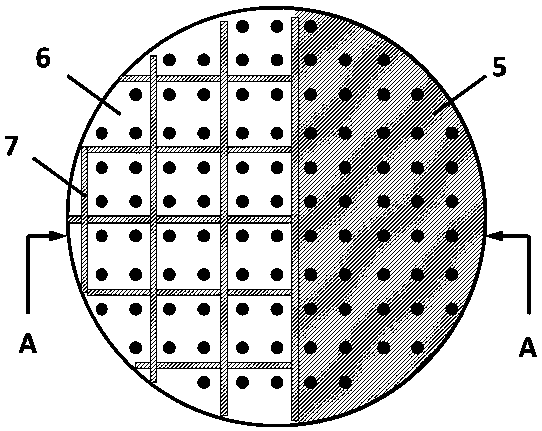
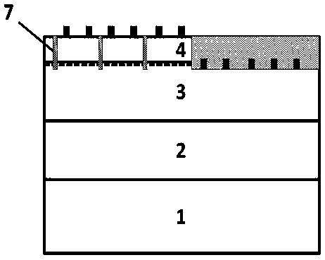
[0032] a. If figure 1 , figure 2 As shown, the surface of the gallium nitride epitaxial barrier layer 4 composed of the substrate 1, the buffer layer 2, the channel layer 3 and the barrier layer 4 is divided into a vertical leakage current test area 5 and a Hall effect test area 6;
[0033] b. Perform photolithography, that is, through standard photolithography processes such as glue coating, development, and exposure, so that the vertical leakage current test area 5 is fully exposed, the Hall effect test area 6 and the isolation area 7 between the square test units are exposed, and the remaining areas are covered Photoresist for protection;
[0034] c. Etching, etch the exposed gallium nitride barrier layer in dry etching equipment such as RIE or ICP, and etch as deep as the channel layer, th...
Embodiment 2
[0043] The gallium nitride epitaxial wafer vertical leakage current and Hall effect combined testing method of the present invention is carried out according to the following steps:
[0044] a. If Figure 4 , Figure 5 As shown, the surface of the gallium nitride epitaxial barrier layer 4 composed of the substrate 1, the buffer layer 2, the channel layer 3 and the barrier layer 4 is divided into a vertical leakage current test area 5 and a Hall effect test area 6;
[0045] b. Perform photolithography, that is, through standard photolithography processes such as glue coating, development, and exposure, so that the vertical leakage current test area 5 is fully exposed, the Hall effect test area 6 electrode deposition area 8 is exposed, and the remaining areas are covered with photoresist. Protect;
[0046] c. Etching, etch the exposed gallium nitride barrier layer in dry etching equipment such as RIE or ICP, and etch as deep as the channel layer, that is, the etching depth exc...
PUM
 Abstract
Description
Claims
Application Information


