Semiconductor wafer lapping method and semiconductor wafer
A grinding method and semiconductor technology, applied in semiconductor devices, semiconductor/solid-state device manufacturing, grinding machine tools, etc., can solve problems such as deterioration of nanometer topography
- Summary
- Abstract
- Description
- Claims
- Application Information
AI Technical Summary
Problems solved by technology
Method used
Image

Examples
Embodiment
[0063] Next, in order to clarify the effects of the present invention, the following examples are given, but the present invention is not limited by the following examples.
[0064] (Invention Example 1)
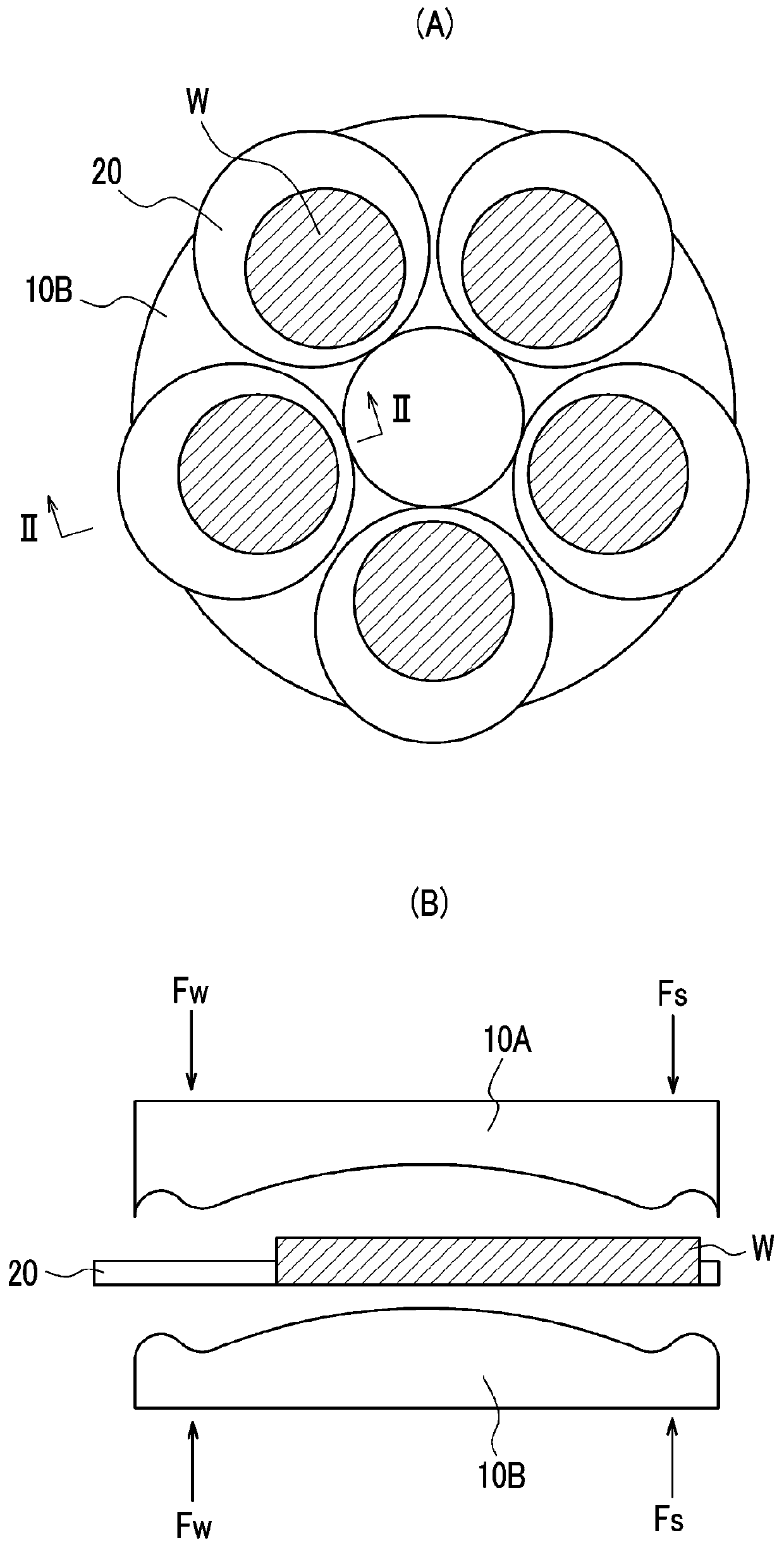
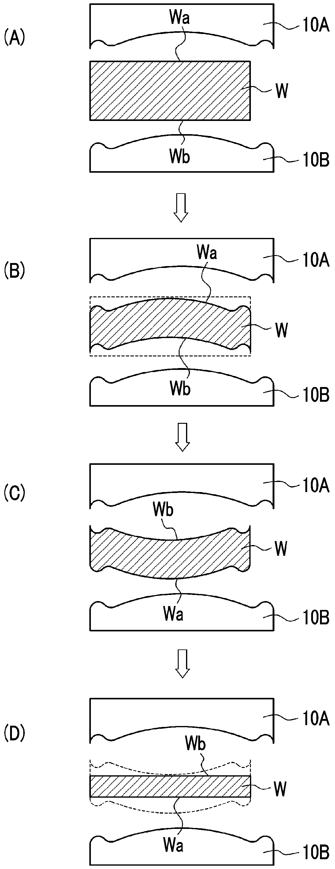
[0065] According to the aforementioned figure 1 structure and Figure 5 In the flowchart shown, the grinding of a silicon wafer with a diameter of 450 mm was carried out. That is, a silicon wafer with a diameter of 450 mm obtained by slicing a single crystal ingot was loaded on a carrier plate and placed between the upper stage and the lower stage of the polishing apparatus. In addition, the total grinding time until the target grinding allowance was obtained was confirmed in advance.
[0066] First, the grinding of the silicon wafer was started and stopped after 35% of the total grinding time had elapsed. After stopping the grinding, use the adsorption pad to remove the silicon wafer from the carrier plate, turn over the silicon wafer opposite to the upper platform and ...
example 1
[0070] A silicon wafer with a diameter of 450 mm was polished in the same manner as Inventive Example 1 except that the polishing was not stopped and the polishing was terminated after the total polishing time had elapsed. That is, in Conventional Example 1, inversion of the silicon wafer and restart of polishing were not performed.
[0071]
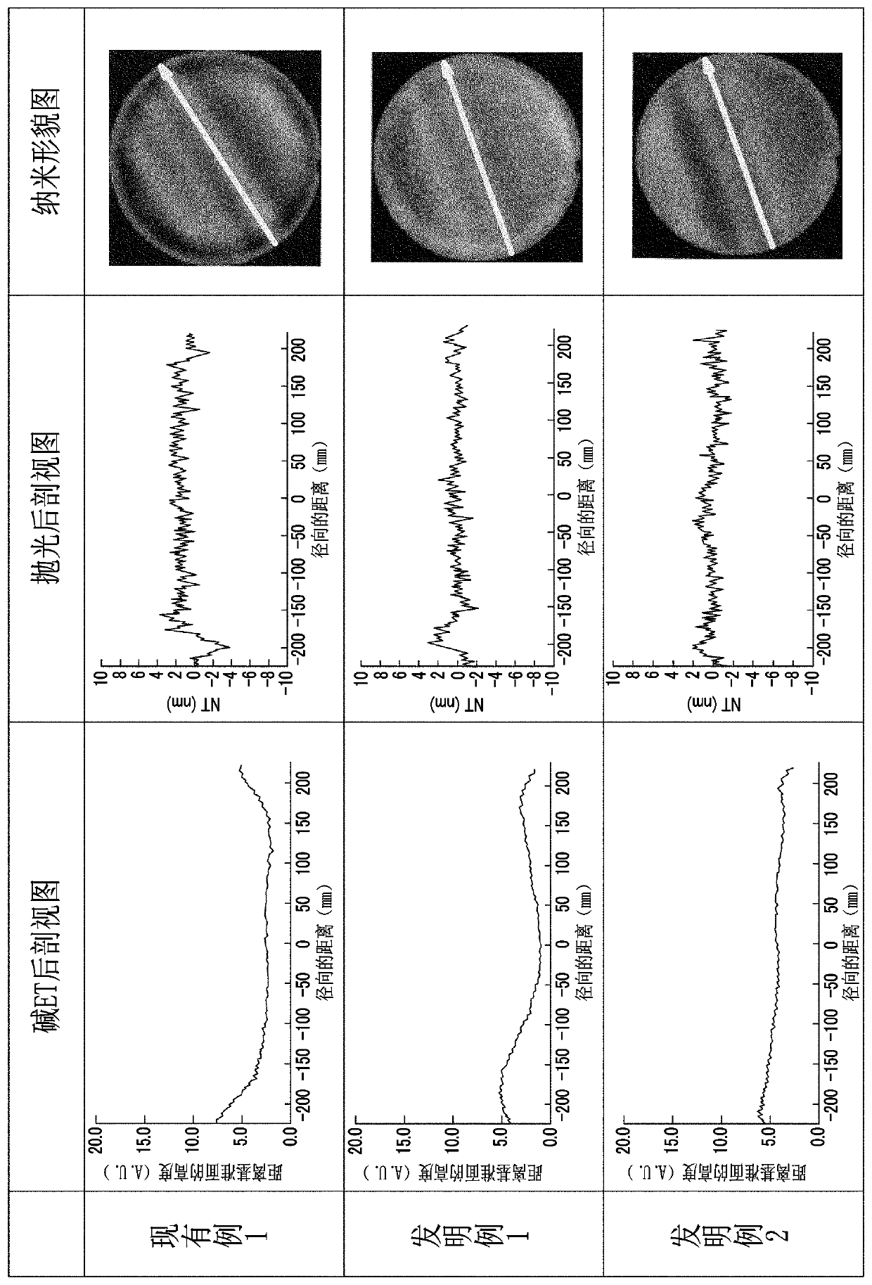
[0072] Alkali etching (hereinafter abbreviated as "alkali ET") was performed on the polished silicon wafers of Invention Examples 1 to 5 and Conventional Example 1 under the same conditions. Then, using a capacitive shape measuring device (manufactured by Kobelco Scientific Research Co., Ltd.; SBW-451 / R), the radial direction of the silicon wafer (the direction of the arrow shown in the nano-topography diagram, which corresponds to the cross-sectional view of the wire saw moving direction) was measured. , so as not to be affected by the ups and downs of slice cutting), the graph of the shape distribution. show the result in Image 6 ...
PUM
| Property | Measurement | Unit |
|---|---|---|
| diameter | aaaaa | aaaaa |
| diameter | aaaaa | aaaaa |
| diameter | aaaaa | aaaaa |
Abstract
Description
Claims
Application Information
 - R&D
- Intellectual Property
- Life Sciences
- Materials
- Tech Scout
- Unparalleled Data Quality
- Higher Quality Content
- 60% Fewer Hallucinations
Browse by: Latest US Patents, China's latest patents, Technical Efficacy Thesaurus, Application Domain, Technology Topic, Popular Technical Reports.
© 2025 PatSnap. All rights reserved.Legal|Privacy policy|Modern Slavery Act Transparency Statement|Sitemap|About US| Contact US: help@patsnap.com