Decapsulation of electronic devices
An electronic device, decapsulation technology, applied in the cleaning/polishing of conductive patterns, circuits, printed circuits, etc.
- Summary
- Abstract
- Description
- Claims
- Application Information
AI Technical Summary
Problems solved by technology
Method used
Image

Examples
example 1
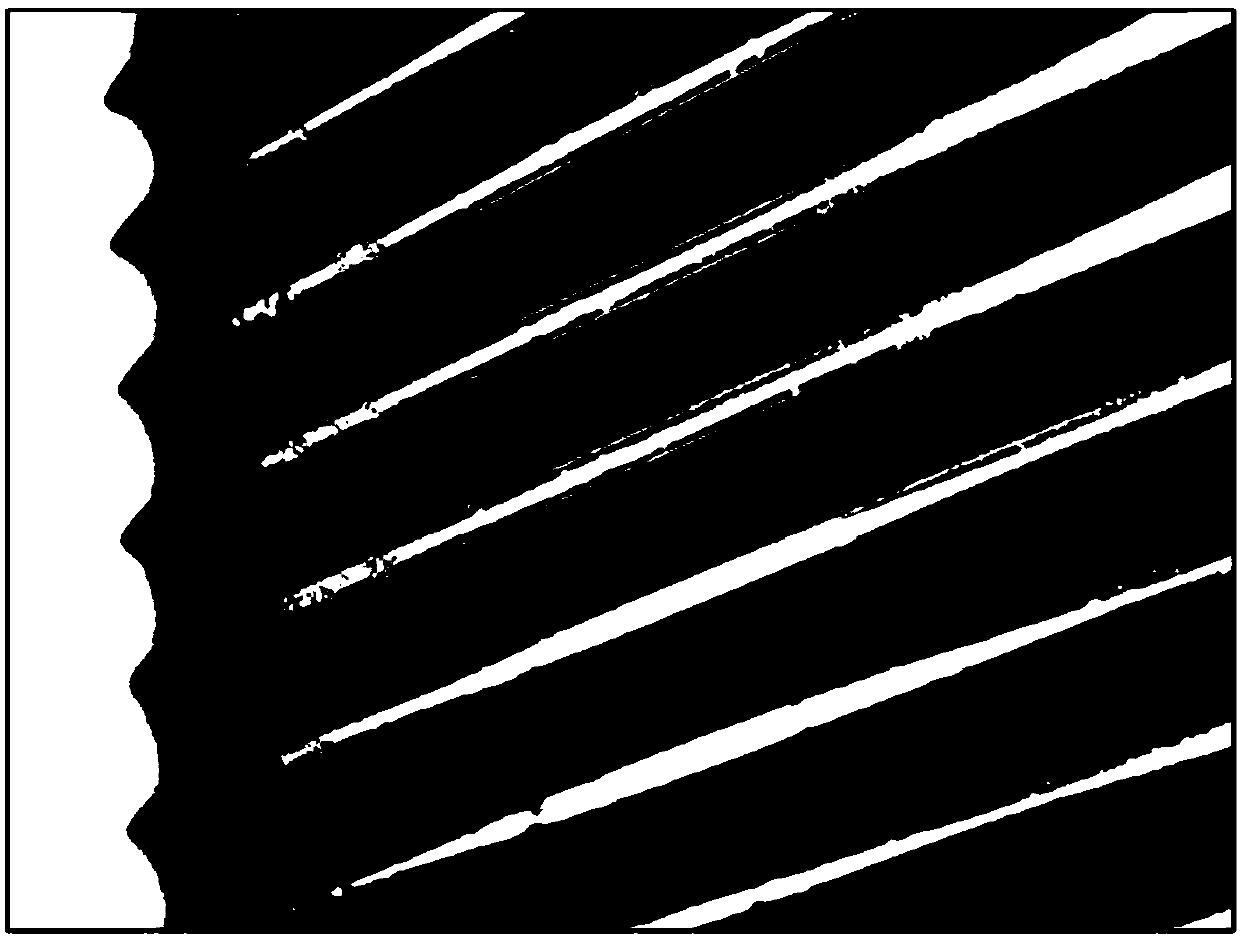
[0047] In a MIP etching apparatus marketed by Jiaco Instruments B.V. (Delft, The Netherlands) and described in WO2013 / 184000, from argon-containing gas with a flow rate of 400 seem using an argon flow of 1400 seem A gas flow induction plasma of gas and hydrogen (95:5). The plasma was combined with ultrasonic cleaning for depackaging semiconductor devices including silver bonding wires and plastic packaging comprising 10% epoxy resin and 90% silicon filler. An unpackaged semiconductor device was obtained which, on visual inspection, showed a clean wire surface ( figure 1 ).
example 2
[0049] Gas flows comprising argon, nitrogen, and hydrogen (i.e., a first flow of argon (100% by volume) at 1400 seem and a second flow of nitrogen and hydrogen (95% by volume and 5% by volume, respectively) at 25 seem were used. Mixture) The experiment described in Example 1 was repeated. An unpackaged semiconductor device was obtained which, upon visual inspection, showed an acceptably clean and slightly damaged silver line surface.
[0050] example comparison
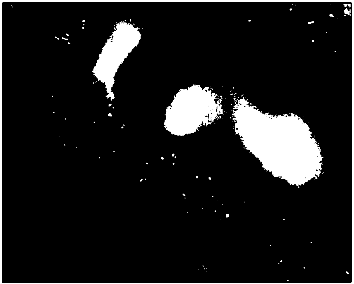
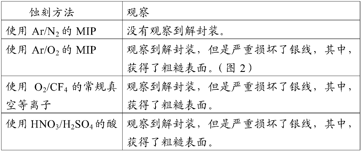
[0051] Use including Ar / N 2 , Ar / O 2 ( figure 2 ), O 2 / CF 4 Repeat the test described in Example 1 (without ultrasonic cleaning), or use the conventional acid decapsulation method to complete the decapsulation. The results are summarized in Table 1.
[0052] Table 1 Example Comparison
[0053]
PUM
 Abstract
Description
Claims
Application Information
 - R&D
- Intellectual Property
- Life Sciences
- Materials
- Tech Scout
- Unparalleled Data Quality
- Higher Quality Content
- 60% Fewer Hallucinations
Browse by: Latest US Patents, China's latest patents, Technical Efficacy Thesaurus, Application Domain, Technology Topic, Popular Technical Reports.
© 2025 PatSnap. All rights reserved.Legal|Privacy policy|Modern Slavery Act Transparency Statement|Sitemap|About US| Contact US: help@patsnap.com