Chip glass packaging process

A technology of glass encapsulation and process, applied in the manufacture of encapsulation/shell resistors, resistor shells/packaging shells/potting, non-adjustable metal resistors, etc., can solve problems such as performance changes, changes, and chip defects, and achieve The effect of enhancing the mechanical strength

Inactive Publication Date: 2019-05-07
ZHAOQING EXSENSE ELECTRONICS TECH
View PDF7 Cites 0 Cited by
  • Summary
  • Abstract
  • Description
  • Claims
  • Application Information

AI Technical Summary

Problems solved by technology

E.g figure 1 As shown, the existing thermistor chip with the upper and lower electrode structure includes a porcelain body 2 and electrodes 21 and 22 respectively arranged on the two surfaces of the porcelain body 2. The chip welding process connects the upper and lower electrodes before packaging, and the chip needs to be soaked in flux before inserting the chip. The flux contains acidic substances, and the acid will corrode the ceramic body 2 of the chip. After the ceramic body 2 is corroded, the resistance value of the chip will change. As a result, its performance also changes, resulting in a decrease in the reliability of the chip
another example figure 2 As shown, the existing thermistor chip with left and right electrode structures includes a porcelain body 20 and electrodes 201 located at both ends of the porcelain body 20. When in use, it is directly attached to the PCB board 60 printed with silver glue. The body 20 has no protection, and a water film will be formed on the surface of the chip in a humid environment to form a surface resistance, such as image 3 As shown, the change of the resistance value of the ceramic body 20 causes the chip performance to change accordingly. After testing, it is found that the thermistor chip with the resistance value of 10KΩ welded to the extension wire is placed in a constant humidity cabinet with a humidity of 90% for 1 hour. After the measurement, its resistance value became 9.980KΩ, indicating that the reliability of the chip decreased in a humid environment
[0003] In addition, the SMD chip and the circuit board are easily bent and deformed by external forces during the assembly process
For example, the thermistor chip will produce micro-cracks along with the deformation of the PCB board 60, resulting in abnormal performance or fracture and directly open circuit, such as Figure 4 As shown, especially when the PCB board and chip are injected in the injection molding process, the extrusion of the PCB board when the injection molding machine is clamping the upper and lower molds will cause micro-cracks or breakage in the ceramic body of the chip, resulting in defective chips (approximately 2% bad), after dismantling the packaging colloid on the bad chip, the resistance test of the chip is often found that the chip is close to an open circuit, and then soldered with an electric soldering iron, the chip is disconnected from the middle
[0004] It can be seen that the existing chip for chip placement and chip insertion has the problems of poor moisture resistance and low mechanical strength

Method used


Image

  • Chip glass packaging process
  • Chip glass packaging process
  • Chip glass packaging process

Examples


Embodiment Construction

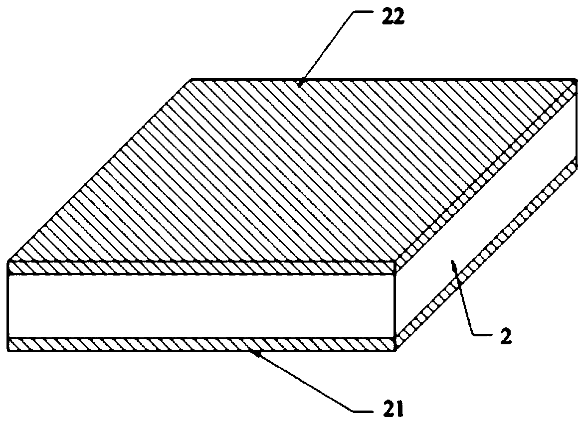
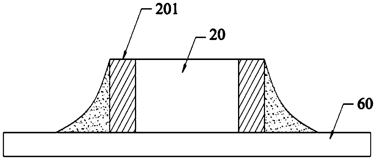
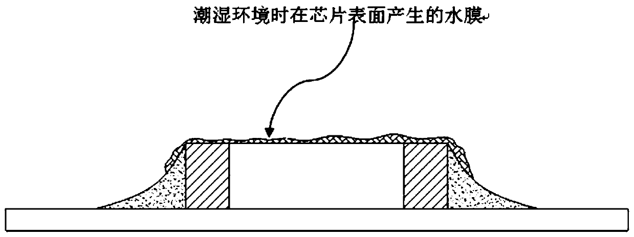
[0027] In the chip glass encapsulation process of the present invention, a layer of glass film is sputtered on the surface of the exposed part of the ceramic body in the thermistor chip to form the encapsulation.

[0028] The ceramic body in the thermistor chip is a cube, and an electrode layer is respectively provided on the top surface and the bottom surface of the ceramic body.

[0029] The thermistor chip can be an existing thermistor chip with upper and lower electrode structures, or a thermistor chip with left and right electrode structures, specifically a chip chip with a model number of 0603, and the electrode layer is a silver layer.

[0030] The process specifically includes the following steps: cover the two electrode layers of the thermistor chip with a high temperature resistant film, then place the thermistor chip in the vacuum coating chamber of the vacuum sputtering coating equipment, and then apply the vacuum coating The chamber is evacuated to -90KPA, and the...


PUM

PropertyMeasurementUnit
thicknessaaaaaaaaaa

Abstract

The invention relates to a chip glass packaging process which comprises sputtering a glass film onto the surface of an exposed portion of a porcelain body in a thermistor chip to form a package. The chip glass packaging process of the present invention significantly enhances the mechanical strength, the moisture resistance and the corrosion resistance of the chip.

Description

technical field [0001] The invention relates to the technical field of electronic components, in particular to a chip glass packaging process. Background technique [0002] At present, there is no encapsulation protection for the exposed part of the ceramic body of the chips used for patching and inserting chips, such as thermistor chips. For example figure 1 As shown, the existing thermistor chip with upper and lower electrode structures includes a porcelain body 2 and electrodes 21 and 22 respectively arranged on the two surfaces of the porcelain body 2. The chip welding process connects the upper and lower electrodes before packaging, and the chip needs to be soaked in flux before inserting the chip. The flux contains acidic substances, and the acid will corrode the ceramic body 2 of the chip. After the ceramic body 2 is corroded, the resistance value of the chip will change. As a result, its performance also changes, resulting in a decrease in the reliability of the ch...

Claims


Application Information

Patent Timeline
Patent Type & Authority Applications(China)
IPC IPC(8): H01C17/02H01C7/00H01C1/02
Inventor 邓意芳段兆祥杨俊柏琪星唐黎民
Owner ZHAOQING EXSENSE ELECTRONICS TECH
Why Eureka
Try Eureka