Silicon wafer alloy process

A technology of alloy technology and silicon wafer, which is applied in the direction of electrical components, semiconductor/solid-state device manufacturing, circuits, etc., can solve the problems of air bubbles in the soldering layer, poor welding of lead-tin solder sheet and silicon wafer, and poor heating of the edge and center of the silicon wafer. To solve the problem of uniformity, achieve the effect of less welding bubbles, save manpower and equipment, and improve product quality and reliability

Inactive Publication Date: 2019-05-14
TIANJIN HUANXIN TECH DEV
View PDF10 Cites 0 Cited by
  • Summary
  • Abstract
  • Description
  • Claims
  • Application Information

AI Technical Summary

Problems solved by technology

[0003] The purpose of the present invention is to solve the problem of uneven heating of the edge and center of the silicon chip in the process of silicon chip alloying in the prior art, resulting in poor welding of the lead-tin solder sheet and the silicon chip after alloying and bubbles in the welding layer, and provides a silicon chip Sheet alloy process

Method used


Image

  • Silicon wafer alloy process

Examples


Embodiment Construction

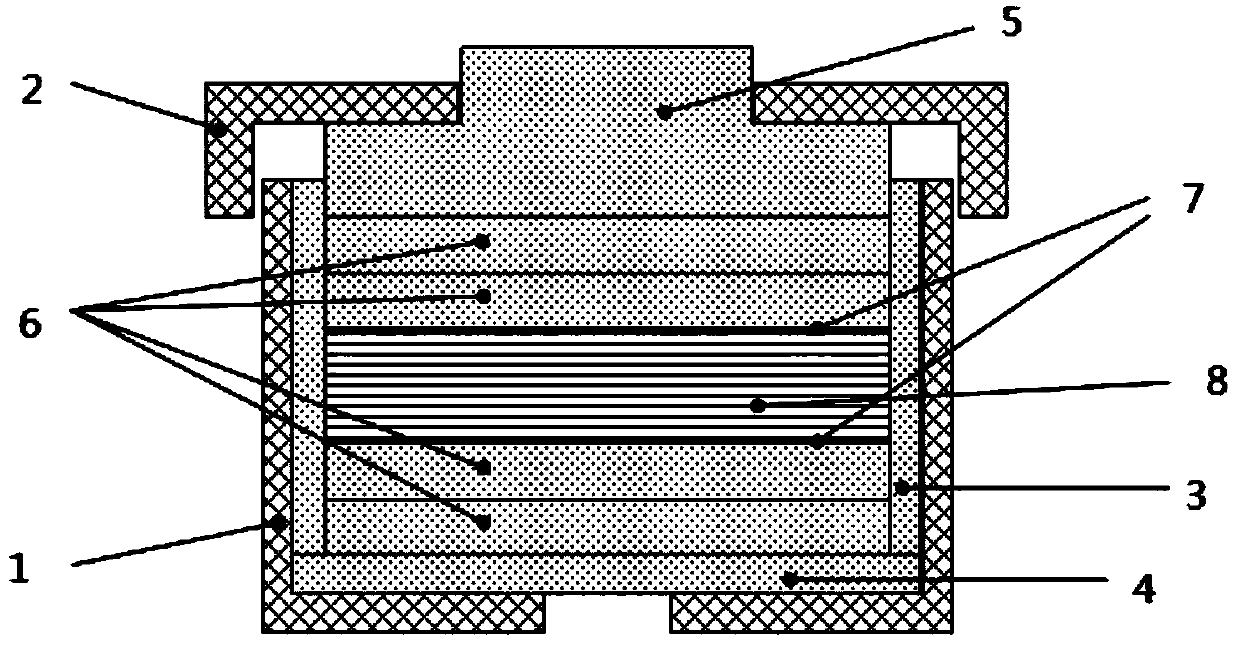
[0034] A silicon wafer alloy process, including sequential primary alloying and secondary alloying, wherein the primary alloying sequentially includes the following steps:

[0035] S11, stacking, stacking a plurality of silicon wafers to form a silicon block, a first soldering piece is provided between every two silicon wafers, and a primary welding piece is also provided at both ends; the specific operation steps are: Put a piece of gold-plated silicon wafer with the N+ side up on the aluminum foil, then put one piece of soldering piece, and then put a piece of gold-plated silicon wafer, that is, press gold-plated silicon wafer-soldering piece-gold-plated silicon wafer-soldering piece... The gold-plated silicon wafers are stacked in sequence. According to this, the gold-plated silicon wafers are stacked alternately with the primary soldering wafers for several times. Note that the N+ type marking surface of the silicon wafers is always placed upwards, and try to keep them in t...


PUM


Abstract

The invention provides a silicon wafer alloy process. The silicon wafer alloy process comprises primary alloying and secondary alloying which are sequentially performed, wherein the primary alloying sequentially comprises the steps of lamination, first-time die loading, pressurization, first-time sintering and first-time de-molding, and the secondary ally sequentially comprises the steps of second-time die loading, pressurization, secondary sintering and secondary de-molding. The silicon wafer alloy process has the beneficial effects that alloying for two times is employed, a silicon wafer anda lead-tin welding material are prevented from deviating during alloying by placing a graphite sleeve ring in a die sleeve, a die cover is placed at the uppermost layer so as to facilitate pressurization by an oil press machine, the contact of the lead-tine welding material and the silicon wafer in alloying is enabled to be smooth, and favorable wettability with the silicon wafer after melting ofthe welding material is ensured.

Description

technical field [0001] The invention belongs to the technical field of semiconductor wafer manufacturing technology, and in particular relates to a silicon wafer alloy technology. Background technique [0002] In the existing alloy process, there is uneven heating of the edge and center of the silicon wafer when the silicon wafer is alloyed, which leads to the problem of poor welding between the lead-tin solder sheet and the silicon wafer after alloying and bubbles in the soldering layer, which affects the follow-up welding yield. In the follow-up process, the chip and lead welding effect is not good, which affects the service life of the product. Contents of the invention [0003] The purpose of the present invention is to solve the problem of uneven heating of the edge and center of the silicon chip in the process of silicon chip alloying in the prior art, resulting in poor welding of the lead-tin solder sheet and the silicon chip after alloying and bubbles in the weldin...

Claims


Application Information

Patent Timeline
Patent Type & Authority Applications(China)
IPC IPC(8): H01L21/603
Inventor 王鹏梁效峰宋楠徐长坡陈澄钟瑜杨玉聪王晓捧
Owner TIANJIN HUANXIN TECH DEV
Why Eureka
Try Eureka