Method for representing defect of two-dimensional material and application thereof

A two-dimensional material and defect technology, applied in the field of characterization of two-dimensional material defects, can solve the problems of small characterization area, low efficiency and high electron beam, and achieve the effect of large characterization area, high efficiency and fast imaging

Active Publication Date: 2019-05-17
TSINGHUA UNIV
View PDF9 Cites 6 Cited by
  • Summary
  • Abstract
  • Description
  • Claims
  • Application Information

AI Technical Summary

Problems solved by technology

[0005] However, these methods have some shortcomings: the electron beam used in the TEM characterization process is relatively high, resulting in new defects, in addition, the characterization area is relatively small, the sample preparation is demanding, the cost is high, and the efficiency is low; the use of Raman to characterize the defect sample For a long time, the laser spot of Raman characterization is on the order of microns, the efficiency is low, and large-area Raman scanning characterization cannot be performed; when using fluorescence spectroscopy to characterize two-dimensional materials, most of them need to be at low temperature (low temperature is sensitive to defects) )conduct

Method used


Image

  • Method for representing defect of two-dimensional material and application thereof
  • Method for representing defect of two-dimensional material and application thereof
  • Method for representing defect of two-dimensional material and application thereof

Examples


Embodiment 1

[0084] Example 1 Detection of WS by fluorescence lifetime imaging 2 defect

[0085] Two-dimensional material WS by mechanical exfoliation 2 Prepared on a release base.

[0086] Prepare samples with defects: use a plasma cleaner to introduce defects into the samples, the power of the plasma cleaner is 20W, the radio frequency is 13.56MH, and the sample is bombarded with argon gas for 10s.

[0087] Use the fluorescence lifetime imaging system (PicoHarp 300, PicoQuant) to perform fluorescence lifetime imaging detection on samples with defects, such as image 3 As shown, the excitation wavelength is 488nm, and the frequency is 40MHz. The objective lens (40X, NA 0.95) is used to focus the laser light to excite the sample. The generated fluorescence signal is collected by the same objective lens. Layer WS 2 The fluorescence lifetime of each spot is filtered, and the filtered optical signal is detected by a photodetector, and then the photodetector and laser are synchronized by a...

Embodiment 2

[0090] Example 2 confirms that defects make fluorescence lifetime longer

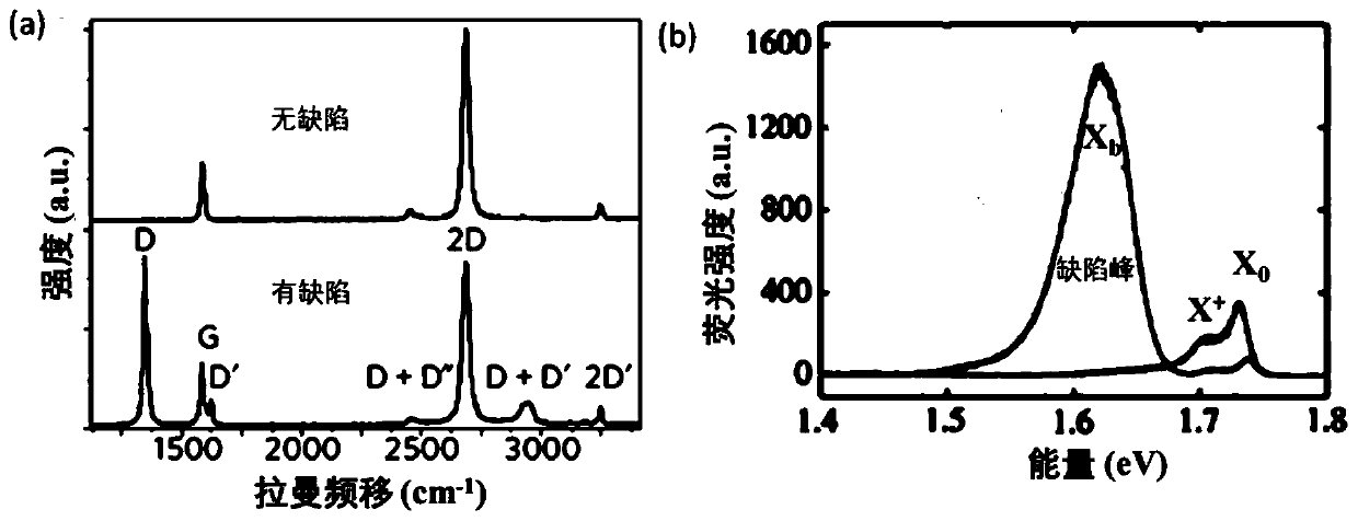
[0091] Raw single layer WS 2 The fluorescence spectrum of Figure 5 As shown, it can be seen that WS before plasma treatment 2 The fluorescence peak is superimposed by the neutral exciton peak and the trion peak, and a new peak appears after plasma treatment, that is, the defect state exciton peak.

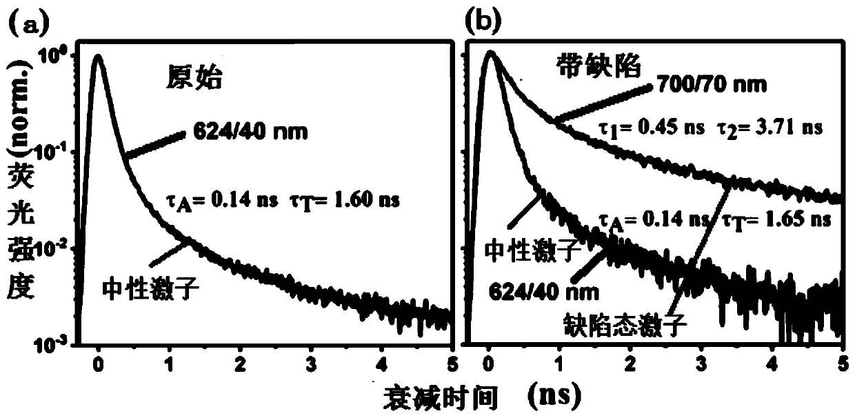
[0092] The time-resolved fluorescence lifetime decay curves for pristine and defect-bearing ones are as Figure 6 shown, from Figure 6 It can be seen that the decay rate of the defect state excitons is significantly reduced, and the fluorescence lifetime is significantly longer, indicating that the defect makes the fluorescence lifetime longer.

[0093] It can be seen that light excitation makes electrons transition from the ground state to the excited state, electrons relax and recombine with holes, and emit photons. When defects exist, defect fluorescence peaks can be generated. The defect fluorescen...

Embodiment 3

[0094] Example 3 Effect of defects on the exciton-exciton annihilation process in monolayer tungsten disulfide

[0095] The presence of defects also causes a decrease in the exciton-exciton annihilation (EEA) rate. Exciton-exciton annihilation is a process in which one exciton transfers energy to another exciton. It is a non-radiative process, so it can shorten the fluorescence lifetime, and the exciton annihilation rate can be obtained through data processing. When the defects exist, the intrinsic excitons in the sample can be bound to form defect state excitons, which will reduce the number of intrinsic excitons, so the number of excitons used to participate in the exciton annihilation process decreases, and the annihilation rate decreases.

[0096] Figure 7 is the effect of different excitons on the exciton-exciton annihilation, Figure 7 In (a) the fluorescence spectrum weights of neutral excitons, trion excitons, and defect state excitons are given as a function of las...


PUM

PropertyMeasurementUnit
Excitation wavelengthaaaaaaaaaa
Frequencyaaaaaaaaaa

Abstract

The invention discloses a method for representing a defect of a two-dimensional material and application thereof, and relates to the technical field of defect representation of a nanomaterial. The method for representing the defect comprises the step of: respectively and independently carrying out fluorescence lifetime imaging on a non-defect two-dimensional material substrate sample and a to-be-detected two-dimensional material substrate sample, and according to the change of a fluorescence lifetime, judging whether the to-be-detected two-dimensional material substrate sample has a defect, i.e., if the fluorescence lifetime of the to-be-detected two-dimensional material substrate sample is longer than that of the non-defect two-dimensional material substrate sample, determining that the to-be-detected two-dimensional material substrate sample is a defect sample, and if the fluorescence lifetime of the to-be-detected two-dimensional material substrate sample has no obvious change withrespect to the fluorescence lifetime of the non-defect two-dimensional material substrate sample, determining that the to-be-detected two-dimensional material substrate sample is a non-defect sample.The method disclosed by the invention adopts a fluorescence lifetime imaging method to represent the defect of the two-dimensional material; by the method, the change of the fluorescence lifetime canbe rapidly and visually observed so as to judge whether the material has the defect; and at the room temperature, representation can be carried out, a new defect cannot be introduced, and the method is a non-destructive detection method.

Description

technical field [0001] The invention relates to the technical field of defect characterization of nanomaterials, in particular to a method for characterizing defects in two-dimensional materials and its application. Background technique [0002] Due to their many unique electrical, optical, chemical and thermal properties, two-dimensional materials are widely used, such as playing a very important role in the construction of microelectronic and optoelectronic components, semiconductor devices and solar cells. At the same time, two-dimensional materials are suitable as a carrier for studying the structure and physical properties of materials, and can also be used as the basic structural unit for constructing other dimensional materials, because the study of two-dimensional materials is very important. [0003] However, it is difficult for two-dimensional materials to exist in large quantities in nature. Generally, they are stripped from natural materials by artificial means o...

Claims


Application Information

Patent Timeline
IPC IPC(8): G01N21/64
CPCG01N21/6408G01N21/6458G01N2021/646G01N21/64
Inventor 刘大猛刘欢王婷雒建斌
Owner TSINGHUA UNIV
Why Eureka
Try Eureka