A kind of impatt diode with double heterojunction and composite passivation layer and its manufacturing method

A technology of double heterojunction and passivation layer, applied in semiconductor devices, electrical components, circuits, etc., to achieve the effect of improving ionization rate, reducing the width of avalanche region, and high breakdown voltage

Active Publication Date: 2020-12-01
XIDIAN UNIV
View PDF4 Cites 0 Cited by
  • Summary
  • Abstract
  • Description
  • Claims
  • Application Information

AI Technical Summary

Problems solved by technology

[0004] However, the main feature of the heterojunction IMPATT diode structure reported so far is the use of different heterojunction materials, such as Si / SiGe heterojunction, n-Si-Ge / p-Ge-Si heterojunction, AlGaAs / GaAs Although the dual-drift region diode structures such as heterojunction and GaAs / GaInP heterojunction reduce the width of the avalanche region to a certain extent and improve the output power and efficiency of the device, the band gap of Si, Ge and GaAs materials is relatively large. small, so that the heterojunction based on these materials still has a certain degree of defects in improving the carrier ionization rate in the avalanche region and limiting the occurrence of the avalanche effect.

Method used


Image

  • A kind of impatt diode with double heterojunction and composite passivation layer and its manufacturing method
  • A kind of impatt diode with double heterojunction and composite passivation layer and its manufacturing method
  • A kind of impatt diode with double heterojunction and composite passivation layer and its manufacturing method

Examples


Embodiment 1

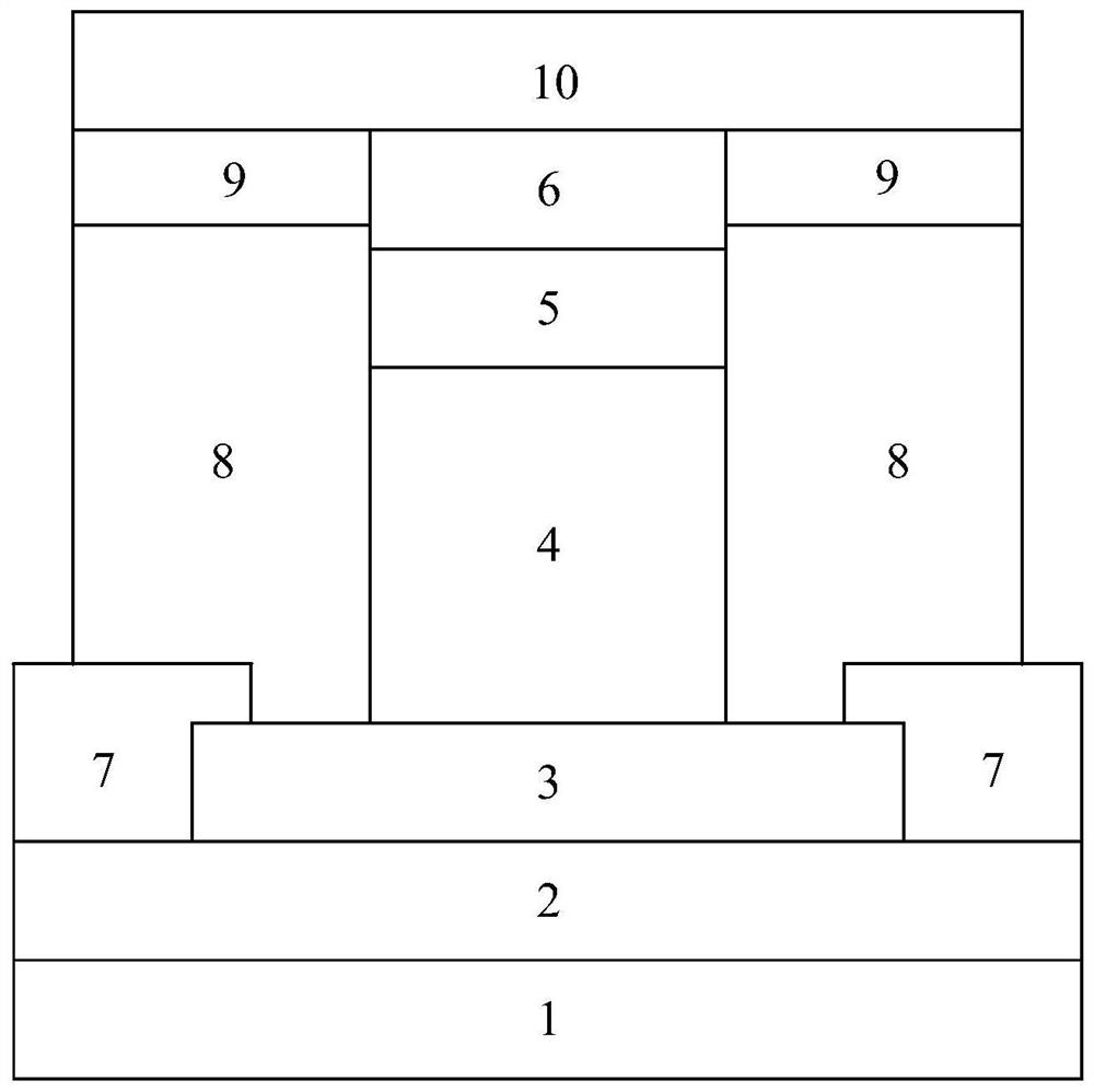
[0050] refer to figure 1 , figure 1 A schematic diagram of an IMPATT diode with a double heterojunction and a composite passivation layer and its preparation method provided by an embodiment of the present invention.

[0051] An IMPATT diode with a double heterojunction and a composite passivation layer provided by an embodiment of the present invention includes:

[0052] substrate layer 1;

[0053] The epitaxial layer 2 is located on the upper layer of the substrate layer 1;

[0054] The ohmic contact layer 3 is located on the upper layer in the middle of the epitaxial layer 1;

[0055] The first drift region 4 is located in the upper layer in the middle of the ohmic contact layer 3;

[0056] The second drift region 5 is located on the upper layer of the first drift region 4;

[0057] Avalanche zone 6, located on the upper floor of the second drift zone 5;

[0058] The ohmic contact electrode 7 is located on both sides of the ohmic contact layer 3 and the upper layer on b...


PUM

PropertyMeasurementUnit
thicknessaaaaaaaaaa
thicknessaaaaaaaaaa
thicknessaaaaaaaaaa

Abstract

The invention relates to an IMPATT diode with double heterojunctions and a composite passivation layer. The IMPATT diode with the double heterojunctions and the composite passivation layer includes asubstrate layer, an epitaxial layer, an ohmic contact layer, a first drift region, a second drift region, an avalanche region, ohmic contact electrodes, a first passivation layer, a second passivationlayer, and a Schottky contact electrode; the epitaxial layer is located on the upper layer of the substrate layer; the ohmic contact layer is located on the upper layer in the middle of the epitaxiallayer; the first drift region is located on the upper layer in the middle of the ohmic contact layer; the second drift region is located on the upper layer of the first drift region; the avalanche region is located on the upper layer of the second drift region; the ohmic contact electrodes are located on both sides of the ohmic contact layer and the upper layer of both sides of the ohmic contactlayer; the first passivation layer is located on the upper layer of the ohmic contact layer and the upper layer of the ohmic contact electrodes, and is located on both sides of the first drift region,on both sides of the second drift region, and on both sides of the avalanche region; the second passivation layer is located on the upper layer of the first passivation layer; and the Schottky contact electrode is located on the upper layer of the avalanche region and the upper layer of the second passivation layer. The IMPATT diode with the double heterojunctions and the composite passivation layer provided by the invention increases the carrier ionization rate in the avalanche region, and the avalanche effect is limited to avalanche region; therefore, the avalanche region width is reduced,and the power output capability is improved.

Description

technical field [0001] The invention belongs to the field of semiconductor technology and semiconductor manufacturing, and in particular relates to an IMPATT diode with a double heterojunction and a composite passivation layer and a manufacturing method thereof. Background technique [0002] In recent years, the third-generation wide-bandgap semiconductors represented by SiC and GaN, because of their large bandgap, high electron saturation drift velocity, high thermal conductivity, high breakdown field strength, strong corrosion resistance and radiation resistance, etc. With excellent physical and chemical properties, it has gradually become the material of choice for making microwave high-power devices. A large number of studies have shown that compared with the traditional III-V compound semiconductor GaAs, the impact ionization avalanche transit time (IMPATT) diode based on GaN material is the most efficient and powerful electronic device among double-terminal solid-state...

Claims


Application Information

Patent Timeline
Patent Type & Authority Patents(China)
IPC IPC(8): H01L31/0304H01L31/0336H01L31/0352H01L31/107
Inventor 杨林安李秀圣马晓华郝跃
Owner XIDIAN UNIV
Why Eureka
Try Eureka