

Lead-free solder alloy comprising sn, bi and at least one of mn, sb, cu and its use for soldering an electronic component to a substrate
A technology of lead-free solder alloy and electronic components, which is applied in the direction of assembling printed circuits, electrical components, welding media, etc. with electrical components, and can solve the problems of electroless nickel plating-gold is not a finish, etc.
- Summary
- Abstract
- Description
- Claims
- Application Information
AI Technical Summary
Problems solved by technology
Method used
Image

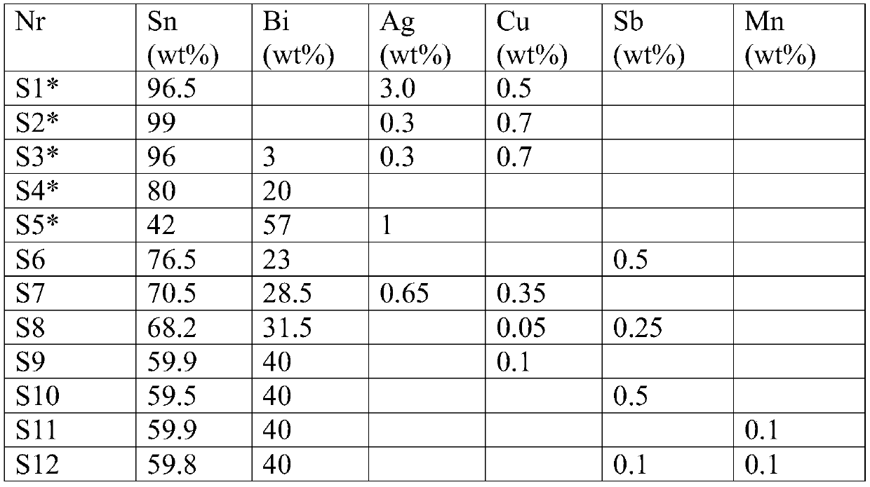
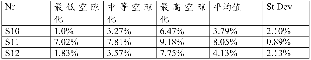
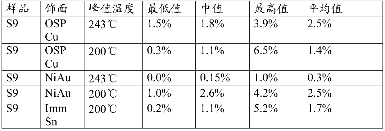
Examples
Embodiment Construction
[0035] To test the reliability, an X-ray analysis is used to test for void formation in so-called QFN packages. A QFN package is a package that has an exposed die pad surrounded by a plurality of contact pads. The QFN package is a popular choice because of its thin and small profile, low weight, and good thermal properties due to the exposed die pad and reduced lead inductance. It is similar to eg QFP (Quad Flat Pack). In 2013, approximately 32.6 billion QFN packages were assembled. Additional variants of the QFN package are most likely to be developed. A QFN package typically includes one or more integrated circuits. A plurality of contact pads are present on all four sides of the package, typically extending on both the sides and the bottom surface of the package. The number of contact pads is for example in the range of 20-100. The pitch (center-to-center distance between adjacent contact pads) is for example in the range of 0.3mm-0.7mm, and the width of the contact pa...
PUM
| Property | Measurement | Unit |
|---|---|---|
| melting point | aaaaa | aaaaa |
Abstract
Description
Claims
Application Information