Package structure comprising at least one transition forming a contactless interface
A packaging structure, non-contact technology, applied in connection devices, semiconductor devices, circuits, etc., can solve the problems of degradation, strong antenna mode interference, high lead inductance, and achieve accurate measurement and promote the effect of measurement
- Summary
- Abstract
- Description
- Claims
- Application Information
AI Technical Summary
Problems solved by technology
Method used
Image
Examples
Embodiment Construction
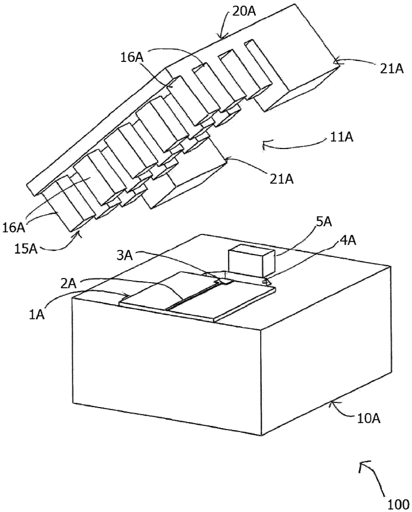
[0063] figure 1 Schematically illustrates a packaging structure 100 comprising an interconnection arrangement comprising a transition between a first transmission line as a microstrip line 2A of a MMIC 1A and a rectangular waveguide 11A according to a first embodiment of the invention . The package structure 100 comprises a waveguide cracked block assembly in which a rectangular waveguide 11A passes through a first conducting block or plate section 10A (here a bottom block), for example solid metal or with a metallized surface, a second conducting (e.g. metal) block or plate section 20A (here the top metal block) and for example metal or metallized longitudinal conductive block connection sections or side walls 21A, 21A formed in The structure 100 is connected to or integral with the second conductive mass section 20A at the waveguide section.
[0064] The package structure 100 as mentioned above comprises a first transmission line comprising a microstrip line 2A of a circu...
PUM
 Abstract
Description
Claims
Application Information


