Packaging structure comprising at least one transition forming contactless interface

A packaging structure, non-contact technology, applied in the direction of connection devices, waveguide devices, electrical components, etc., can solve the problems of strong interference of antenna mode, degradation, impedance mismatch, etc., to achieve the effect of promoting measurement and accurate measurement

Active Publication Date: 2019-05-21
GAPWAVES
View PDF3 Cites 9 Cited by
  • Summary
  • Abstract
  • Description
  • Claims
  • Application Information

AI Technical Summary

Problems solved by technology

[0007] The problem associated with wire bonding at high frequencies is that the wire inductance can be quite high, causing impedance mismatches
The pattern of the antenna cannot be de-embedded from all unwanted radiation from the probe or connector
The structure supporting the antenna and probe or connector causes strong interference on the measured antenna pattern
Furthermore, the probe will radiate significantly as a result of the discontinuity due to the transition between the probe tip and the microstrip line, affecting and degrading the signal-to-noise ratio, dynamic range

Method used


Image

  • Packaging structure comprising at least one transition forming contactless interface
  • Packaging structure comprising at least one transition forming contactless interface
  • Packaging structure comprising at least one transition forming contactless interface

Examples


Embodiment Construction

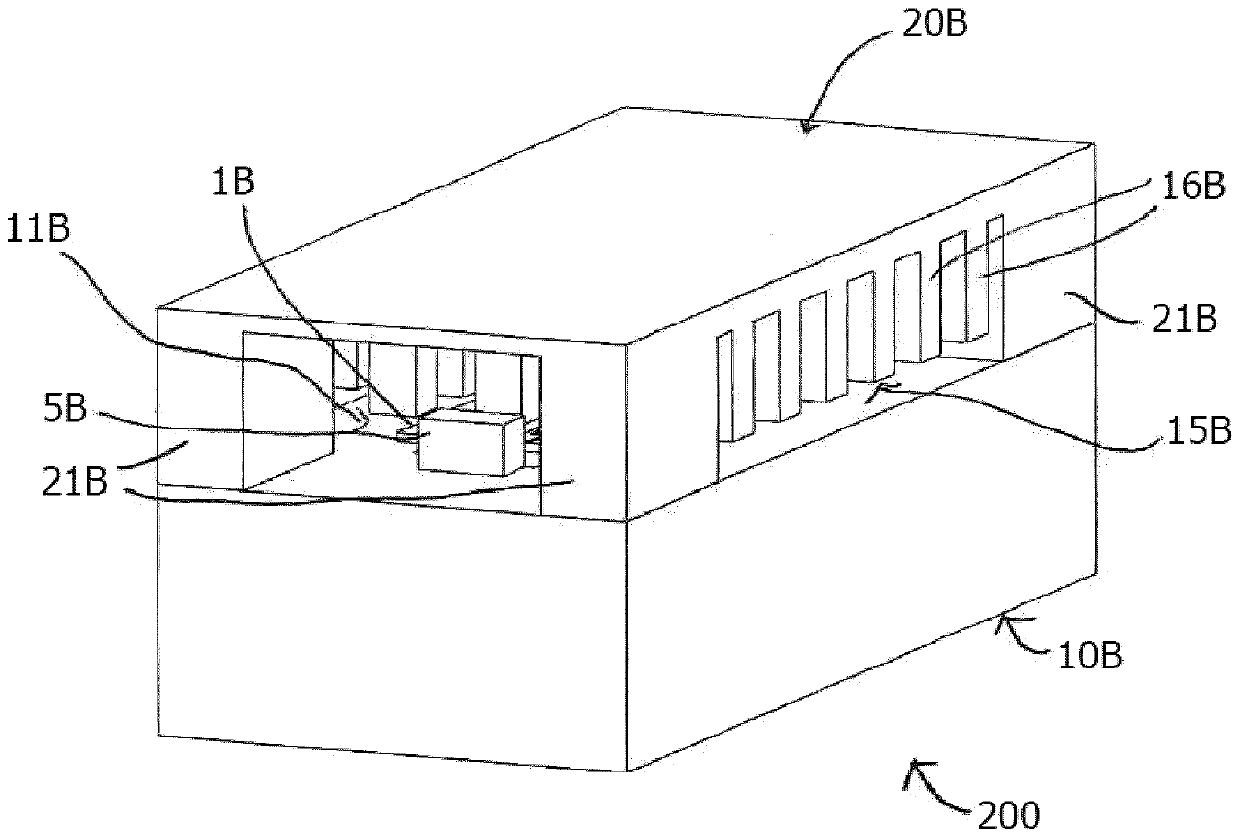
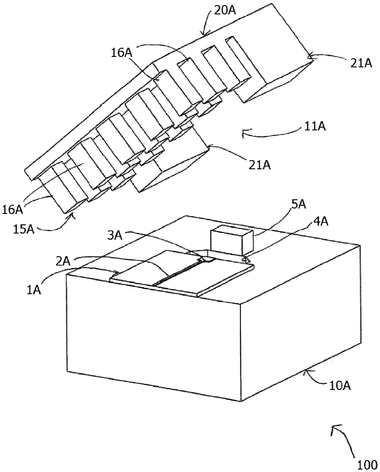
[0063] figure 1 Schematically illustrates a packaging structure 100 comprising an interconnection arrangement comprising a transition between a first transmission line as a microstrip line 2A of a MMIC 1A and a rectangular waveguide 11A according to a first embodiment of the invention . The package structure 100 comprises a waveguide cracked block assembly in which a rectangular waveguide 11A passes through a first conducting block or plate section 10A (here a bottom block), for example solid metal or with a metallized surface, a second conducting (e.g. metal) block or plate section 20A (here the top metal block) and for example metal or metallized longitudinal conductive block connection sections or side walls 21A, 21A formed in The structure 100 is connected to or integral with the second conductive mass section 20A at the waveguide section.

[0064] The package structure 100 as mentioned above comprises a first transmission line comprising a microstrip line 2A of a circu...


PUM


Abstract

The present invention relates to a packaging structure (100)comprising a split-block assembly with a first and a second conducting block section (10A, 20A) and at least one transition between a firstplanar transmission line (2A) and a second transmission line (11A), and one or more input / output ports. The first transmission line (2A) is arranged on a substrate, e.g. an MMIC (1A), disposed on thefirst conducting block section (10A) and comprises a coupling section (3A), the first conducting block (10A) comprises a cavity (4A) with a cavity opening in an upper surface of the first conducting block section (10A) so arranged that, in an assembled state of the split-block assembly, the coupling section (3A) will be located above, or in, the opening of the cavity (4A), the second transmissionline (11A) being in line with the first transmission line (2A) and located on an opposite side of the opening of the cavity (4A).The second conducting block section (20A) acts as a lid in an assembledstate of the packaging structure. One of the conducting block sections is provided with a high impedance surface (15A) in a transition region along or facing the first (2A) and second (11A) transmission lines, a narrow gap being provided between the high impedance surface region (15A) and the opposing surface of the other conducting block section (10A) at least in the transition region such thatthe transition will be contactless without any galvanic contact between the first and second transmission lines (2A, 11A).

Description

technical field [0001] The invention relates to an encapsulation structure having the features of the first part of claim 1, said encapsulation structure comprising at least one transition between a first transmission line and a second transmission line. [0002] The invention also relates to an interconnection device comprising a contactless transition having the features of the first part of claim 31 . [0003] The invention also relates to the use of an interconnect arrangement as claimed in claim 33 for performing measurements on a device comprising an electronic circuit or a device under test (DUT). Background technique [0004] In the mmWave and submillimeterWave frequency bands, the use of high frequencies is receiving increasing attention. Being able to use millimeter or submillimeter wave frequency regions is attractive because larger frequency bandwidths are available in these frequency regions. Thus, transitions or interconnections between circuits and waveguide...

Claims


Application Information

Patent Timeline
Patent Type & Authority Applications(China)
IPC IPC(8): H01P5/107
CPCH01P5/107H01L23/66H01L2223/6633H01L2223/6677H01L2223/6683
Inventor A.U.扎曼J.杨U.南迪
Owner GAPWAVES
Why Eureka
Try Eureka