Testing device for a memory chip in a hybrid circuit

A memory chip and test device technology, applied in static memory, instruments, etc., can solve problems such as hard-to-fail memory fault location and diagnosis, functional test vector development and debugging difficulties, and the inability to directly apply hybrid integrated circuits, etc., to achieve easy test generation , the effect of small test vector size and small external resource overhead

Active Publication Date: 2019-05-24
XIAN MICROELECTRONICS TECH INST
View PDF5 Cites 6 Cited by
  • Summary
  • Abstract
  • Description
  • Claims
  • Application Information

AI Technical Summary

Problems solved by technology

However, how to conduct effective high-coverage testing for memory chips in hybrid circuit forms to verify the manufacturing defects introduced by the assembly process of hybrid integrated circuits for memory is a problem faced in the circuit test verification stage
[0003] MBIST (Memory Build in Self Test) is an industry-recognized excellent test solution for single-chip embedded memory, but it cannot be directly applied to hybrid integrated circuits. For hybrid circuit memory chips, more functions are read in the traditional sense. Test it with write access
However, this method has the following problems: First, the function access method is realized by writing memory-related control registers, the control timing is relatively complicated, the generation of test vectors is difficult, and the judgment of the memory readout result is not intuitive; Second, the specific structure of the memory determines that there are various related fault modes such as fixation, coupling, and address decoding, and the functional access is limited by the functional behavior of the processor or the main controller. It is difficult to target the fault type of the memory according to a specific algorithm. , to generate test vectors with high test coverage, but the test coverage is insufficient; third, the development and debugging of functional test vectors is more difficult, and the test time and test cost are higher
Furthermore, the functional test access method is difficult to locate and diagnose faulty memory

Method used


Image

  • Testing device for a memory chip in a hybrid circuit
  • Testing device for a memory chip in a hybrid circuit
  • Testing device for a memory chip in a hybrid circuit

Examples


Embodiment Construction

[0018] The technical solution of the present invention will be further described below in conjunction with the accompanying drawings and specific embodiments.

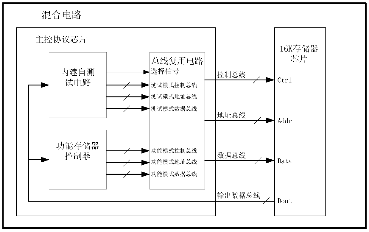
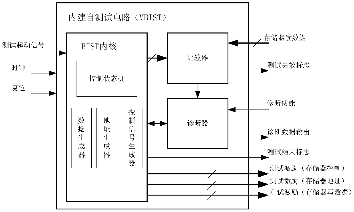
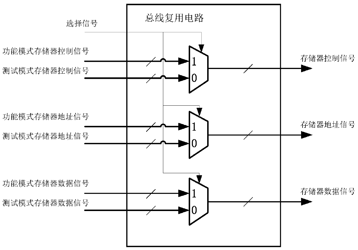
[0019] The invention provides a test device for a memory chip in a hybrid circuit. The device utilizes the characteristics of data interaction between the memory chip and the main control protocol chip in the hybrid circuit, designs a built-in self-test circuit in the main control chip of the hybrid circuit, and multiplexes The function data and the control bus are used to realize the test access to the memory chip. The test device mainly includes a built-in self-test circuit and a bus multiplexing circuit.

[0020] Such as figure 1 As shown, the device includes a built-in self-test circuit, a functional memory controller and a bus multiplexing circuit, and the built-in self-test circuit, a functional memory controller and a bus multiplexing circuit are arranged on the main control protocol chip; at the same time, the ...


PUM


Abstract

The invention provides a testing device for a memory chip in a hybrid circuit. capable of achieving fault positioning and diagnosis at the same time; The device comprises a built-in self-test circuitand a bus multiplexing circuit. The built-in self-test circuit and the bus multiplexing circuit are arranged on the main control protocol chip; The built-in self-test circuit is connected with a selection signal port of the bus multiplexing circuit. The built-in self-test circuit is connected with the bus multiplexing circuit through the test mode control bus, the test mode address bus and the test mode data bus. The main control protocol chip also comprises a functional memory controller; Wherein a control bus of the main control protocol chip is connected with a control port of the memory chip, a data bus of the main control protocol chip is connected with a data port of the memory chip, and an address bus of the main control protocol chip is connected with an address port of the memorychip; An output data bus of the main control protocol chip is connected with an output data port of the memory chip; And the built-in self-test circuit and the functional memory controller read data on the memory chip through the output data bus.

Description

technical field [0001] The invention belongs to the technical field of memory chip testing, and in particular relates to a testing device for memory chips in a hybrid circuit. Background technique [0002] Due to its high assembly density, high reliability, and good electrical performance, hybrid integrated circuit technology is widely used in many fields such as computers, automobiles, communications, and aerospace. However, how to perform effective high-coverage testing on memory chips in a hybrid circuit form to verify the manufacturing defects introduced by the assembly process of the hybrid integrated circuit to the memory is a problem faced in the circuit test verification stage. [0003] MBIST (Memory Build in Self Test) is an industry-recognized excellent test solution for single-chip embedded memory, but it cannot be directly applied to hybrid integrated circuits. For hybrid circuit memory chips, more functions are read in the traditional sense. Test it with write ...

Claims


Application Information

Patent Timeline
Patent Type & Authority Applications(China)
IPC IPC(8): G11C29/14G11C29/56
Inventor 李俊玲沈拉民颜伟屈博强
Owner XIAN MICROELECTRONICS TECH INST
Why Eureka
Try Eureka