
Memory and forming method thereof

A memory and storage structure technology, which is applied in the manufacturing of electric solid-state devices, semiconductor devices, semiconductor/solid-state devices, etc., can solve the problems of complex process flow, long cycle and high process cost in the contact part of the wafer, and improve the lateral isolation performance. , the effect of improving quality and reducing the difficulty of forming

Active Publication Date: 2019-05-28
YANGTZE MEMORY TECH CO LTD
View PDF6 Cites 2 Cited by
  • Summary
  • Abstract
  • Description
  • Claims
  • Application Information

AI Technical Summary

Problems solved by technology

[0004] In the prior art, the process flow for forming the through-wafer contact part is complex and the cycle is long, resulting in high process cost

Method used


Image

  • Memory and forming method thereof
  • Memory and forming method thereof
  • Memory and forming method thereof

Examples


Embodiment Construction

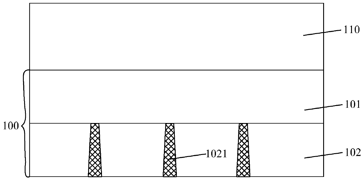
[0028] Please refer to Figures 1A to 1D , is a schematic diagram of the formation process of a semiconductor structure.

[0029] Please refer to Figure 1A , the base 100 includes a substrate 101 and a device layer 102, the substrate 101 includes two opposite surfaces respectively being the front and the back; the device layer 102 is formed on the front of the substrate 101, and the device layer 102 An interconnection structure 1021 is formed in it; after thinning the back of the substrate 101 , a dielectric layer 110 is formed on the back of the substrate 101 .

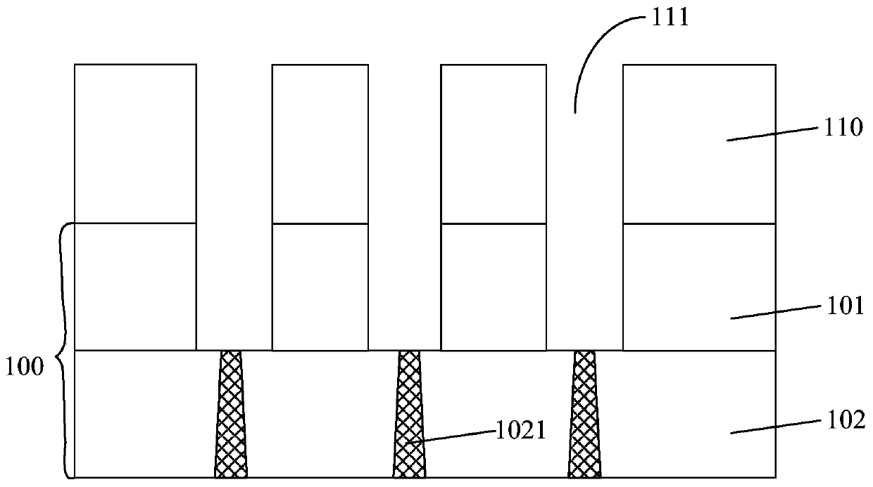
[0030] Please refer to Figure 1B , etching the dielectric layer 110 and the substrate 101 to form a through hole 111 penetrating through the dielectric layer 110 and the substrate 101 , and the interconnection structure 1021 is exposed at the bottom of the through hole 111 .

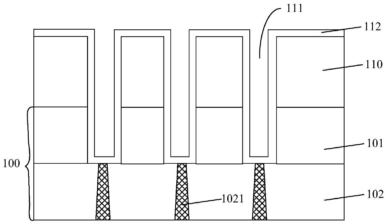
[0031] Please refer to Figure 1C , forming the isolation layer 112 covering the inner wall surface of the through hole 111 .

[0032] P...


PUM


Abstract

The invention relates to a memory and a forming method thereof. The formation method of the memory comprises the following steps of: providing a storage substrate, wherein the storage substrate comprises a substrate and a device layer; the device layer is formed on the front surface of the substrate; a storage structure and an interconnection structure are formed in the device layer; the interconnection structure is electrically connected with the storage structure; an insulating layer is formed in the substrate; at least part of the interconnection structure is formed on the surface of the insulating layer; the top surface of the insulating layer is flush with the front surface of the substrate; and the bottom surface of the insulating layer is flush with the back surface of the substrate; forming a dielectric layer positioned on the back surface of the substrate and the bottom surface of the insulating layer; and forming a through contact part penetrating through the dielectric layerand the insulating layer, wherein the through contact part is electrically connected with at least part of the interconnection structure. The method can save the process steps and reduce the cost.

Description

technical field [0001] The invention relates to the technical field of semiconductors, in particular to a memory and a forming method thereof. Background technique [0002] In recent years, the development of flash memory (Flash Memory) is particularly rapid. The main feature of flash memory is that it can keep stored information for a long time without power on, and has the advantages of high integration, fast access speed, easy erasing and rewriting, etc. Has been widely used. In order to further increase the bit density (Bit Density) of the flash memory while reducing the bit cost (Bit Cost), three-dimensional flash memory (3D NAND) technology has been developed rapidly. [0003] The 3D NAND flash memory structure includes a memory array structure and a CMOS circuit structure above the memory array structure. The memory array junction and the CMOS circuit structure are usually formed on two different wafers, and then bonded to The CMOS circuit wafer and the memory arra...

Claims


Application Information

Patent Timeline
Patent Type & Authority Applications(China)
IPC IPC(8): H01L21/768H01L23/48
Inventor 肖亮陈赫
Owner YANGTZE MEMORY TECH CO LTD
Learn More