COB package and preparation method thereof

A technology for mounting parts and LED chips, applied in climate sustainability, semiconductor devices, electrical components, etc., can solve problems such as thermal failure of the light conversion layer, achieve mass production, simple packaging steps, and improve thermal failure and temperature too high effect

Active Publication Date: 2019-05-28
GUANGZHOU LEDTEEN OPTOELECTRONICS CO LTD
View PDF13 Cites 2 Cited by
  • Summary
  • Abstract
  • Description
  • Claims
  • Application Information

AI Technical Summary

Problems solved by technology

[0005] In order to overcome the deficiencies in the prior art, the first object of the present invention is to provide a COB package, through the improvement of the material of the light

Method used


Image

  • COB package and preparation method thereof
  • COB package and preparation method thereof
  • COB package and preparation method thereof

Examples


Embodiment 1

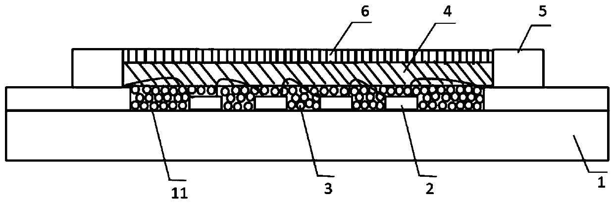
[0053] refer to figure 1 , a COB package, including a substrate 1, an LED chip 2, a light conversion layer 3, a silica gel layer 4, an adhesive barrier 5 and an outer protective layer 6; the substrate 1 is provided with a recessed installation part 11; the depth of the depression of the installation part 11 is 0.3mm; LED chip 2 is fixed in the mounting part 11; light conversion layer 3 covers LED chip 2; silica gel layer 4 is stacked on the top of light conversion layer 3; glue blocking 5 extends upward from substrate 1 and is arranged around silica gel layer 4 The light conversion layer 3 includes methyl silicone rubber; the silicone layer 4 includes methyl silicone rubber; the refractive index of methyl silicone rubber is 1.42, and the hardness is 50shoreA; the outer protective layer 6 is stacked on the top of the silicone layer 4; the outer protective layer 6 Including phenyl silicone rubber; the refractive index of phenyl silicone rubber is 1.5, and the hardness is 65shore...

Embodiment 2

[0058] The COB package of Example 1 is prepared by the following method:

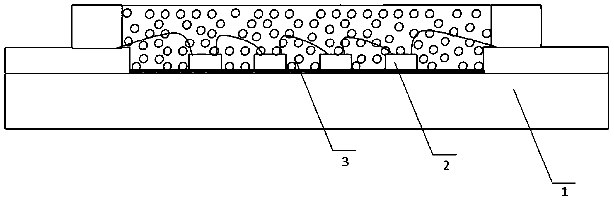
[0059] LED chip fixing step: fix the LED chip in the mounting part of the substrate, and electrically connect the LED chip with a gold wire;

[0060] Steps for forming glue stop: dot coating on the periphery of the LED chip to form a stop glue, the height of the stop glue is 0.5mm, the function of the stop glue is mainly to prevent the light conversion layer from flowing out when filling;

[0061] Light conversion layer filling steps: fill the light conversion layer to cover the LED chip, generally the maximum thickness of the light conversion layer is 0.45mm, and then place it horizontally for 3 hours; the levelness requires ±0.1°;

[0062] Silicone layer filling steps: fill the silicone layer inside the rubber barrier and above the light conversion layer;

[0063] Degassing and baking steps: After filling the silica gel layer, perform defoaming treatment, and then bake, baking in stages: the temperat...


PUM

PropertyMeasurementUnit
Depth of depressionaaaaaaaaaa
Emission wavelengthaaaaaaaaaa
Thicknessaaaaaaaaaa

Abstract

The invention discloses a COB package and a preparation method thereof. The COB package comprises a substrate, an LED chip, a light conversion layer, a silica gel layer and blocking glue. The LED chipis installed on the substrate. The light conversion layer wraps the LED chip. The light conversion layer comprises at least one of methyl silicone rubber and methyl phenyl silicone rubber. The preparation method comprises the following steps: fixing the LED chip; forming the blocking glue blocking: forming the blocking glue on the periphery of the LED chip; filling and coating the light conversion layer: filling and coating the light conversion layer to coat the LED chip, and then standing; filling and coating the silica gel layer: filling and coating the silica gel layer in the blocking glueand on the light conversion layer; performing defoaming and baking: after the silica gel layer is filled and coated, performing defoaming treatment, and then performing baking. Through material improvement of the light conversion layer, absorbed heat can be rapidly conducted out, and the problems that the light conversion layer loses efficacy due to heating and glue cracks are caused by too hightemperature are effectively solved.

Description

technical field [0001] The invention relates to a COB package and a preparation method thereof, belonging to the technical field of lighting structures. Background technique [0002] Light-emitting diode (LED) is an electroluminescent device processed by semiconductor manufacturing technology. It is widely used in various fields, including backlight units, automobiles, electrical signals, traffic lights, and lighting devices. It is known as an alternative to fluorescent lamps and incandescent lamps. The fourth generation lighting source of the lamp. [0003] The mainstream commercial white LEDs currently on the market are realized by using blue LED chips plus one or more of yellow phosphor, green phosphor, and red phosphor. Specifically, the blue light emitted by the LED chip under the current drive excites the phosphor , so that it produces visible light in other bands, which is mixed with blue light to form white light. At present, LED packaging forms are mainly divided ...

Claims


Application Information

Patent Timeline
IPC IPC(8): H01L33/50H01L33/56
CPCY02B20/00
Inventor 陈智波苏佳槟马丽诗林晓敏
Owner GUANGZHOU LEDTEEN OPTOELECTRONICS CO LTD
Why Eureka
Try Eureka