Packaging structure and packaging method of chip module and wafer level chip

A wafer-level chip and packaging method technology, applied in the structural details of semiconductor lasers, laser components, semiconductor lasers, etc., can solve the problem of inability to meet smaller apertures and high aspect ratios, affecting product conductivity reliability, and limited effective contact area and other problems, to achieve the effect of increasing the effective contact area, shortening the packaging process, and reducing the delamination of edge materials

Active Publication Date: 2021-10-22
华天慧创科技(西安)有限公司
View PDF6 Cites 0 Cited by
  • Summary
  • Abstract
  • Description
  • Claims
  • Application Information

AI Technical Summary

Problems solved by technology

Among them, through-hole processing on the wafer is the core of TSV technology. There are two main types, one is deep reactive ion etching, and the other is laser drilling; deep reactive ion etching technology must rely on thick film lithography technology , pre-formed through-hole patterns on the wafer surface, the cost is high; laser drilling technology cannot meet the production of through-holes with smaller aperture (<10μm) and high aspect ratio
Because some wafers such as VCSEL wafers are not suitable for laser drilling, and the pads in the wafer are small in size and thin in thickness, the effective contact area of ​​the circuit is very limited, which affects the reliability of the product's electrical conductivity.
Moreover, there are too many types of materials located at the cutting line, and problems such as edge material delamination, product splits, and cutting edge chipping may occur

Method used


Image

  • Packaging structure and packaging method of chip module and wafer level chip
  • Packaging structure and packaging method of chip module and wafer level chip
  • Packaging structure and packaging method of chip module and wafer level chip

Examples


Embodiment 1

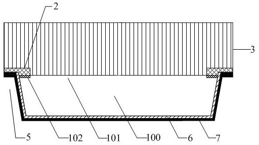
[0044] Such as Figure 1a As shown, a chip module includes a chip unit 100, several metal bumps 2 and optical components 3, the chip unit 100 has a functional surface and a non-functional surface opposite to the functional surface, and the functional surface includes a functional area 101 and a Several welding pads 102 around the functional area; each metal bump 2 is correspondingly formed above each welding pad 102 of the chip unit 100; the optical component 3 and the metal bump 2 and the functional surface of the chip unit 100 not covered by the metal bump 2 Bonding connection: On both sides of the chip unit 100 extending from the non-functional surface to the direction of the metal bump 2, a first opening 5 is formed, the first opening 5 cuts through and exposes the side wall of the solder pad 102, and the bottom of the first opening 5 penetrates to the metal bump 2. The inside of the protrusion 2; the side surface of the first opening 5 and the non-functional surface of th...

Embodiment 2

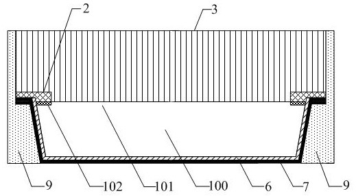
[0052] Such as Figure 2a As shown, a wafer-level chip packaging structure includes a wafer 100', a plurality of metal bumps 2 and a bonding sheet of an embossed element 3'. In this embodiment, the wafer 100' is a VCSEL (Vertical Cavity SurfaceEmitting Laser) wafer.

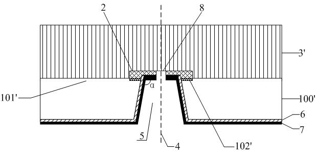
[0053] The wafer 100' has a functional surface and a non-functional surface opposite to the functional surface. The functional surface includes a functional area 101' and a number of pads 102' located around the functional area 101'; the wafer 100' includes a number of chip units. There is a dicing line 4 between two adjacent chip units, and several welding pads 102' of the adjacent two chip units are located on both sides of the dicing line, and the metal bump 2 is formed above the welding pads 102' of the adjacent two chip units. 2 is coaxial with the dicing line 4; the embossing element 3' is bonded to the metal bump 2 and the functional surface of the wafer 100' not covered by the metal bump; the non-functio...

Embodiment 3

[0063] A packaging method for a wafer-level chip, comprising the following steps:

[0064] (1) Wafer preparation: see image 3 , provide a wafer 100' with a plurality of chip units, the wafer 100' has a functional surface and a non-functional surface opposite to the functional surface, the functional surface includes a functional area 101' and several pads 102' located around the functional area.

[0065] (2) Metal bump formation: see Figure 4 , forming a metal bump 2 above the bonding pads 102' of two adjacent chip units. The specific method for forming the metal bump 2 is: first coat a layer of photoresist on the functional surface of the wafer, expose, develop, cover The photoresist in the area of ​​the bonding pads of the two adjacent chip units is developed, and then the metal bump 2 is deposited on the area above the bonding pads 102 ′ of the adjacent two chip units, and finally the remaining photoresist is removed.

[0066] (3) Embossed component bonding: see Figur...


PUM


Abstract

The invention provides a chip module, a wafer-level chip packaging structure and a packaging method. The packaging structure forms metal bumps above the pads of two adjacent chip units. Since the size of the metal bumps is larger than the size of the pads , the thickness is thicker, which increases the effective contact area between the follow-up circuit in the chip unit and the conductive wiring layer, and improves the conductive reliability of the chip packaging structure; one of the technical solutions of the present invention is to directly emboss the optical element on the surface of the wafer The device simplifies two processes into one process, shortens the packaging process, and reduces production costs; the first opening is formed by cutting from the non-functional surface of the wafer to the metal bump direction, which is suitable for wafers that are not suitable for laser drilling Material; and a pre-cutting step is set before the cutting step, so that only the embossed components need to be cut during the cutting step, which reduces the problems of edge material delamination, product slivers, broken knives, and edge collapse during the cutting process.

Description

technical field [0001] The invention relates to the technical field of semiconductor packaging, in particular to a chip module, a wafer-level chip packaging structure and a packaging method. Background technique [0002] The wafer-level chip packaging process based on TSV (Through Silicon Via) technology is to make holes on the non-functional surface of the wafer substrate. The opening extends from the non-functional surface of the wafer to the functional surface of the wafer, and exposes Welding pads on the functional surface, laying metal lines on the inner wall of the opening, leading the electrical properties of the pads to the non-functional surface of the wafer, after preparing bumps on the non-functional surface, cutting to form a single chip packaging structure. Among them, through-hole processing on the wafer is the core of TSV technology. There are two main types, one is deep reactive ion etching, and the other is laser drilling; deep reactive ion etching technolog...

Claims


Application Information

Patent Timeline
Patent Type & Authority Patents(China)
IPC IPC(8): H01S5/183H01S5/02
Inventor 李凡月
Owner 华天慧创科技(西安)有限公司
Why Eureka
Try Eureka