A light emitting diode and a manufacturing method thereof
A technology of light-emitting diodes and light-emitting layers, applied in electrical components, circuits, semiconductor devices, etc., can solve problems such as current congestion and low carrier mobility, increase adhesion, reduce light absorption efficiency, and improve light extraction efficiency Effect
- Summary
- Abstract
- Description
- Claims
- Application Information
AI Technical Summary
Problems solved by technology
Method used
Image

Examples
Embodiment 1
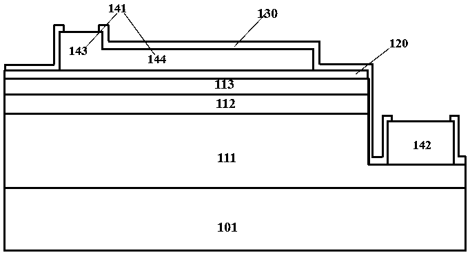
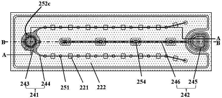
[0082] see Figure 3-5 ,in image 3 shows a top view of a light emitting diode according to a first preferred embodiment of the present invention, Figure 4 is along image 3 A side sectional view taken along the line A-A, Figure 5 is along image 3 A side sectional view taken along the line B-B. The LED comprises: a substrate 201 , an N-type layer 211 , a light-emitting layer 212 , a P-type layer 213 , an insulating layer 221 , a transparent conductive layer 230 , a protective layer 222 , a first electrode 241 , and a second electrode 242 . The first electrode 241 includes a pad 243 and an extension 244 , and the second electrode 242 includes a pad 245 and an extension 246 .
[0083] Specifically, the substrate 201 includes but is not limited to sapphire, aluminum nitride, gallium nitride, silicon, and silicon carbide, and its surface structure can be a planar structure or a patterned pattern structure; the N-type layer 211 is formed on the sapphire substrate 201 the l...
Embodiment 2
[0098] Figure 9 with 10 A schematic diagram showing the structure of another light-emitting diode, where Figure 9 for top view, Figure 10 along Figure 9 Sectional view cut by line A-A. The difference from Embodiment 1 is that in the light emitting diode structure described in this embodiment, the insulating layer 221 under the first electrode 241 is connected together, so that the current injection under the electrode can be completely avoided, and the height of the first electrode extension part 244 can be reduced. All of them are raised, and the refraction effect can be used to effectively reduce the metal light blocking area of the electrode extension, thereby improving the light extraction efficiency of the LED.
Embodiment 3
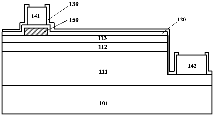
[0100] Figure 11-12 A schematic diagram of the structure of another light-emitting diode is shown, where Figure 11 for top view, Figure 12 along Figure 11 Sectional view cut by line A-A. The difference from Embodiment 1 is that in the light-emitting diode structure described in this embodiment, under the extension portion 244 of the first electrode, the insulating layer 221 overlaps with the opening 251 of the protective layer 222, wherein the area of the insulating layer 221 is smaller than that of the opening. 251 square meters. Figure 13 It shows a partially enlarged view of the extension 244 of the first electrode. The transparent conductive layer 230 forms a gap between the opening 251 and the protective layer 222. The extension 244 of the first electrode fills the gap. On the one hand, the first electrode is in the insulating layer. The position of 221 forms a nail pile structure, which increases the adhesion between the electrode extension 244 and the protect...
PUM
 Abstract
Description
Claims
Application Information
 - R&D
- Intellectual Property
- Life Sciences
- Materials
- Tech Scout
- Unparalleled Data Quality
- Higher Quality Content
- 60% Fewer Hallucinations
Browse by: Latest US Patents, China's latest patents, Technical Efficacy Thesaurus, Application Domain, Technology Topic, Popular Technical Reports.
© 2025 PatSnap. All rights reserved.Legal|Privacy policy|Modern Slavery Act Transparency Statement|Sitemap|About US| Contact US: help@patsnap.com