Selective absorption emitter

An emitter, selective technology, used in refrigerators, lighting and heating equipment, refrigeration and liquefaction, etc., can solve problems such as limitations, increase the complexity of experimental equipment and manufacturing costs, and achieve the effect of low precision requirements

Active Publication Date: 2019-06-07
NINGBO INST OF MATERIALS TECH & ENG CHINESE ACADEMY OF SCI
View PDF11 Cites 7 Cited by
  • Summary
  • Abstract
  • Description
  • Claims
  • Application Information

AI Technical Summary

Problems solved by technology

In 2015, Australia's Min Gu research team reported in Advanced Optical Materials (volume 3, page 1047) an infrared thermal emitter based on a hyperbolic metamaterial, which has an average emissivity of 0.8 in the atmospheric transparent window, higher than 0.67 for the multilayer film system, however, the researchers did not test the passive r...

Method used


Image

  • Selective absorption emitter
  • Selective absorption emitter
  • Selective absorption emitter

Examples


Embodiment 1

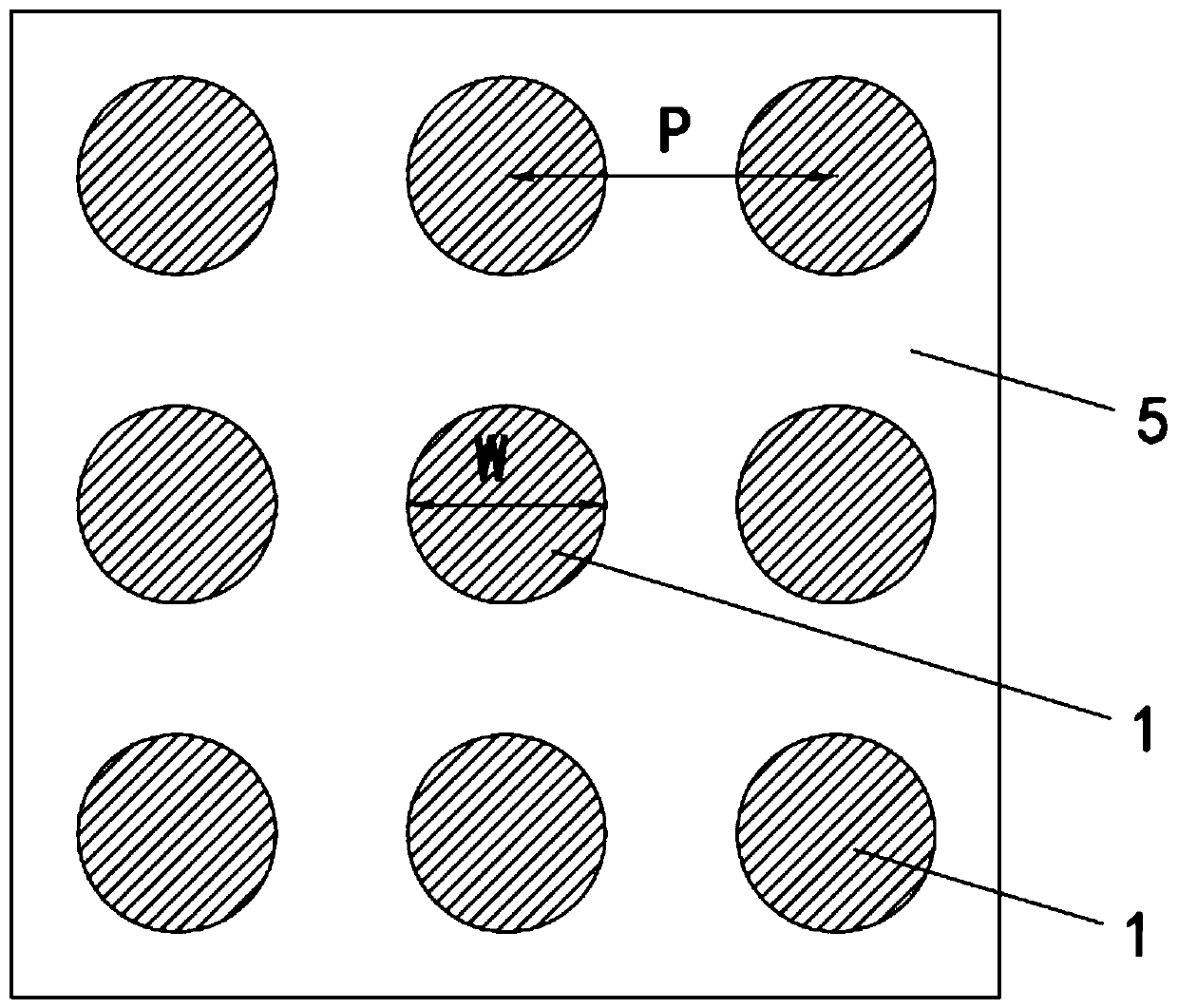
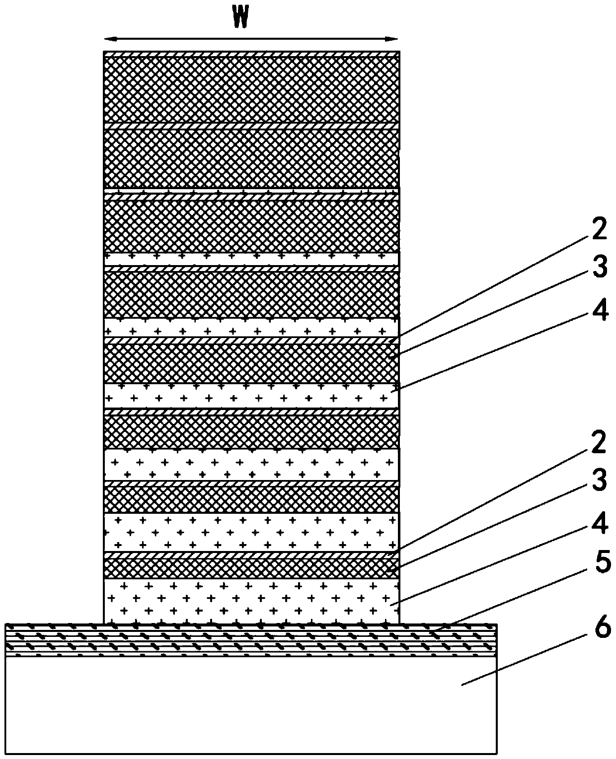
[0032] The selectively absorbing emitter of embodiment 1, such as figure 1 As shown, it includes a substrate 6, a metal film 5 covered on the substrate 6, and a vertical cylindrical two-dimensional periodic cell array arranged on the metal film 5. Each basic unit 1 is composed of 8 stacks stacked sequentially from top to bottom, and each stack includes a metal layer 2 and two dielectric layers with different refractive indices located on the lower side of the metal layer 2, that is, the upper and lower The first dielectric layer 3 and the second dielectric layer 4 are set, and the angle between the side of each basic unit 1 and the normal line of the substrate 6 is 0°, that is, the basic units 1 forming the cell array in this embodiment are all cylindrical .

[0033] In Embodiment 1, the schematic diagram of the structural connection between a single basic unit 1 and the substrate 6 is as follows figure 2 As shown, its period P=5μm, cylinder diameter W=3μm. The metal thin ...

Embodiment 3

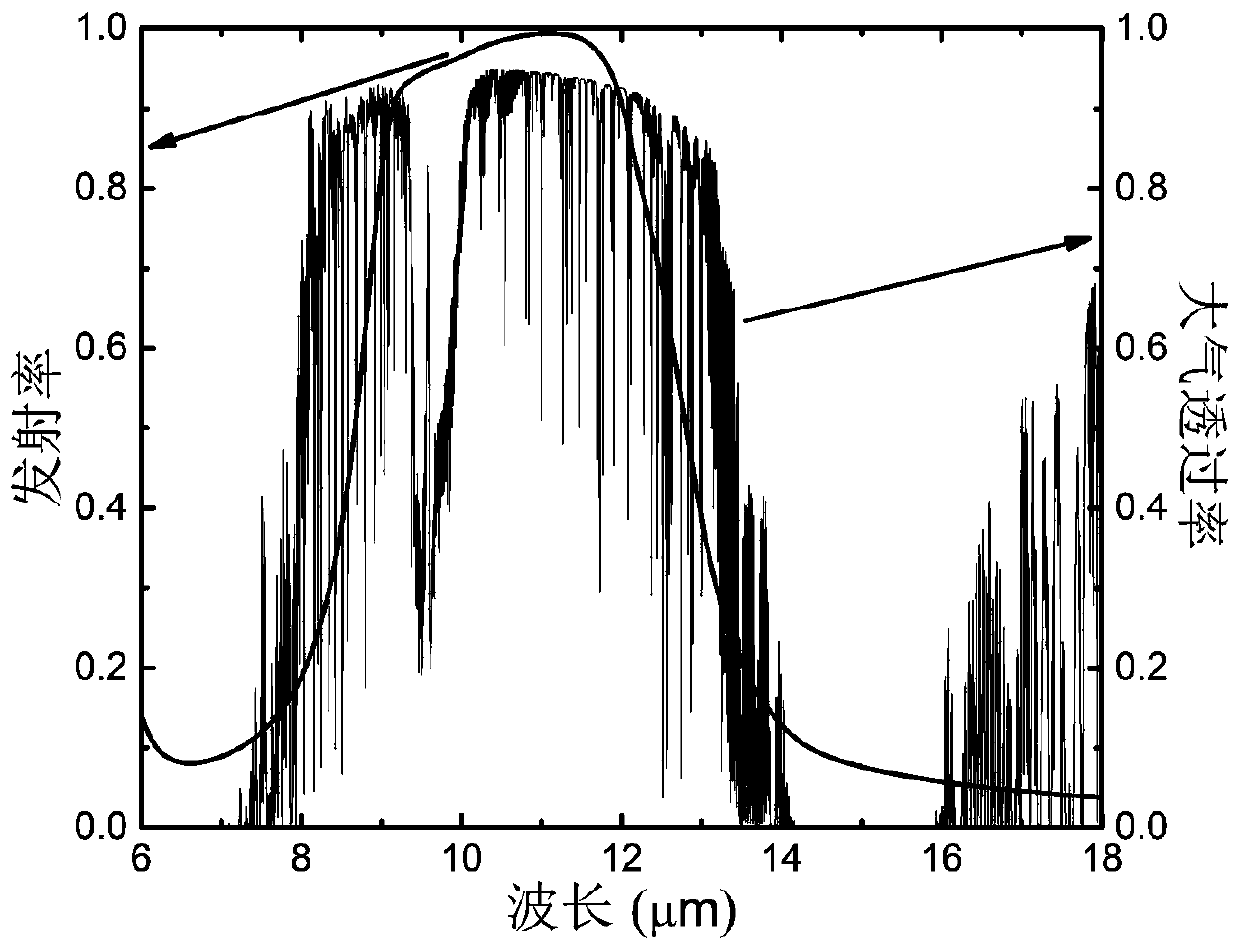
[0039] Example 3 is another case of experimental error. The difference between the selective absorption emitter of embodiment 3 and embodiment 1 is that in embodiment 3, the angle θ between the side surface of each basic unit 1 and the normal line of the substrate 6 is a negative value. Figure 7 It is the emissivity spectrum of the selective absorption emitter of embodiment 3 when there is this angle. The schematic diagram of the longitudinal section of a single basic unit 1 is shown as Figure 7 As shown in the inset below the middle curve, the top dimension of base unit 1 is larger than the bottom dimension. From Figure 7 It can be seen from the middle curve that with the increase of the absolute value of the included angle θ, the emissivity of the selective absorbing emitter at the wavelength of the 8-13 μm atmospheric transparent window decreases, and the bandwidth also decreases, but it still has a good selective absorbing emission characteristic.

[0040] In additi...


PUM


Abstract

The invention discloses a selective absorption emitter. The selective absorption emitter comprises a substrate, a metal film covering the substrate and a cell array arranged on the metal film, whereinthe unit array is composed of a plurality of basic units which are arranged at intervals and have the same shape and the same size, each basic unit is composed of a plurality of stacks which are sequentially stacked from top to bottom, each stack comprises a metal layer and a dielectric layer located on the lower side of the metal layer or two dielectric layers with different refractive indexes,and the included angle between the side surfaces of the basic units and the normal of the substrate is minus 80-80 degrees. The selective absorption emitter is a broadband absorption emitter with wavelength selectivity. The correlation degree between the working wavelength of the emitter and the diameter or the length of the tops and the bottoms of the basic units in the unit array is small, the requirement on the precision of preparation technology is low, when the working wavelength of the emitter ranges from 8 microns to 13 microns, and high absorption and high emissivity are achieved, theemitter can be used for passive radiation refrigeration, and the required absorption characteristics can be obtained in other wavelength ranges by changing array design parameters.

Description

technical field [0001] The invention belongs to the field of photoelectric and photothermal functional materials and devices, and in particular relates to a selective absorption emitter. Background technique [0002] Kirchhoff's thermal radiation law is used to describe the relationship between the emissivity and absorptivity of an object, which states that at the same temperature, the ratio of the monochromatic radiation flux density to the monochromatic absorptivity of different objects for the same wavelength is the same as the The monochromatic radiation flux density of a black body at the same wavelength is equal at temperature, that is, the absorptivity is equal to the emissivity. It shows that the more radiating an object is, the more absorbing it is, and vice versa. [0003] Thermal radiation is a non-contact heat transfer method, which relies on electromagnetic wave radiation to achieve energy transfer between hot and cold objects, even in a vacuum. In 2014, the r...

Claims


Application Information

Patent Timeline
IPC IPC(8): F25B23/00
Inventor 宋伟杰林昇华鲁越晖徐云飞娄雪勤
Owner NINGBO INST OF MATERIALS TECH & ENG CHINESE ACADEMY OF SCI
Why Eureka
Try Eureka