Avalanche photodiode optimized based on photonic crystal broadband total reflector

An avalanche photoelectric and photonic crystal technology, which is applied in the field of photodetectors, can solve the problems of difficulty in designing a total reflector, high reflectivity, low reflection efficiency, etc., and achieves the effect of increasing quantum efficiency and responsivity and improving performance.

Inactive Publication Date: 2019-06-07
南京科普林光电科技有限公司
View PDF0 Cites 1 Cited by
  • Summary
  • Abstract
  • Description
  • Claims
  • Application Information

AI Technical Summary

Problems solved by technology

One is to use a metal electrode as the reflective layer, but its high near-infrared absorption rate and the uneven surface caused by the alloy cause scattering, resulting in low reflection efficiency; the other is to add a distributed Bragg reflector with high reflectivity (distributedBragg reflection, DBR) , but the fixed optical thickness of its structure and the limitation of materials lead to a generally small high reflectivity spectrum, and it is difficult to design a total reflector that can just cover the full optical communication band (1310-1675nm) with a wide spectrum and different incident angles

Method used


Image

  • Avalanche photodiode optimized based on photonic crystal broadband total reflector
  • Avalanche photodiode optimized based on photonic crystal broadband total reflector
  • Avalanche photodiode optimized based on photonic crystal broadband total reflector

Examples


Embodiment Construction

[0022] In order to make the object, technical solution and advantages of the present invention clearer, the present invention will be described in further detail below in conjunction with specific embodiments and with reference to the accompanying drawings.

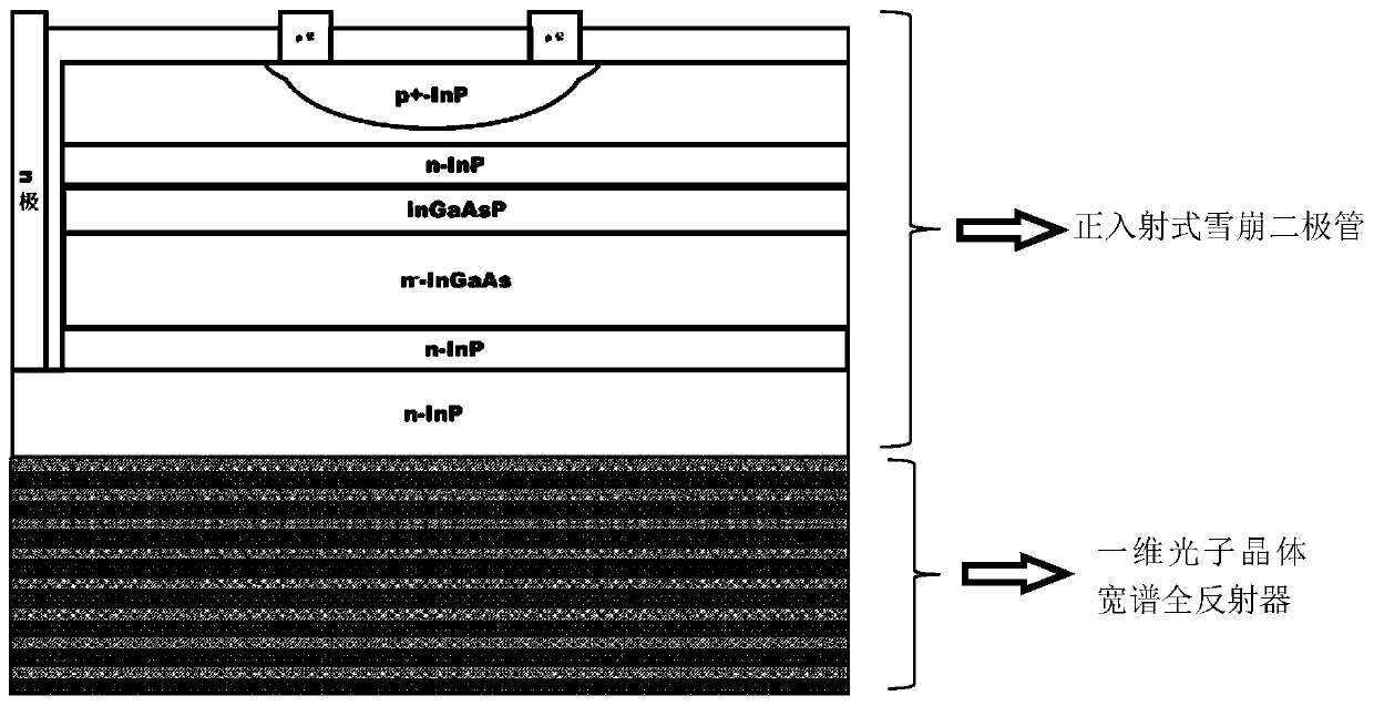
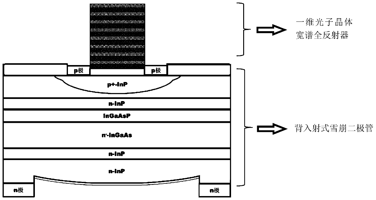
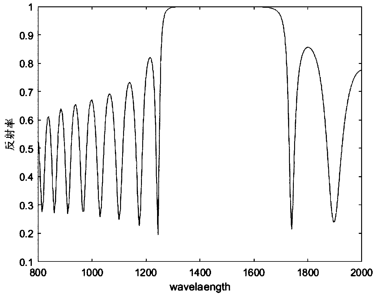
[0023] When manufacturing high-frequency response avalanche diodes, the smaller thickness w of the absorbing layer causes part of the incident light to be absorbed and utilized by the absorbing layer, while part of the light exits the device, so that part of the light information is not used, resulting in a lower quantum efficiency : 40-50%. The lower device quantum efficiency leads to lower device responsivity: 0.52-0.61A / W.

[0024] Devices often use metal electrodes as reflectors to improve light utilization efficiency, but metal electrodes have low reflection efficiency due to their high infrared absorption rate and surface unevenness caused by alloys, which does not improve the quantum efficiency of devices.

[0025...


PUM


Abstract

The present invention discloses an avalanche photodiode optimized based on a photonic crystal broadband total reflector and a manufacturing method thereof. The avalanche photodiode is a one-dimensional photonic crystal broadband total reflector alternately formed by multiple layers of SiO2 dielectric films and TiO2 dielectric films at the back surface of the substrate of a normal incidence avalanche photodiode or the front surface of a back incidence avalanche photodiode. The one-dimensional photonic crystal broadband total reflector reflects light which is not absorbed by an absorption layerin the incident light back to the absorption layer in the avalanche photodiode for absorption again. Compared to a current avalanche photodiode, the one-dimensional photonic crystal broadband total reflector is added to reflect the light which is not absorbed by the absorption layer back to the absorption layer for secondary absorption for all the incident light with different angles with opticalcommunication wave bands of 1310-1675nm without influence of the device frequency response so as to increase the quantum efficiency and responsivity of the device and improve about 50% performances ofthe device.

Description

technical field [0001] The invention relates to the technical field of photodetectors, in particular to an optimized avalanche photodiode based on a photonic crystal wide-spectrum total reflector and a manufacturing method thereof. Background technique [0002] With the development of optoelectronic technology, high-frequency, low-noise and high-sensitivity avalanche photodiodes (Avalanche Photodiodes, APD) are increasingly being used in high-bit-rate, long-distance optical fiber communication systems. Among them, the APD detector with InGaAs / InP absorption, gradient, charge, multiplication (Separate Absorption, Grading, Charge and Multiplication, SAGCM) structure, its composition material In 0.53 Ga 0.47 The forbidden band width of As is 0.75ev, and the absorption coefficient reaches 10 in the wavelength range of 1-1.7 microns. 4 cm -1 , where the absorption coefficient at 1550nm is 0.67*10 4 cm -1 . [0003] When manufacturing an avalanche diode with high-frequency r...

Claims


Application Information

Patent Timeline
Patent Type & Authority Applications(China)
IPC IPC(8): H01L31/107H01L31/0232
Inventor 王亮张博健许凯秦金
Owner 南京科普林光电科技有限公司
Why Eureka
Try Eureka