Method for Measuring Medium Surface Roughness Using Confocal Laser Scanning Microsystem

A technology of laser scanning and microscopic systems, which is applied in the direction of measuring devices, optical devices, and material analysis through optical means, can solve problems such as irregular space shape detection, medium structure damage, difficulties, etc., and achieve suitable high precision Measuring, increasing productivity, cost-saving effects

Active Publication Date: 2021-07-02
CHANGCHUN UNIV OF SCI & TECH +1
View PDF0 Cites 2 Cited by
  • Summary
  • Abstract
  • Description
  • Claims
  • Application Information

AI Technical Summary

Problems solved by technology

[0005] In order to solve the problems existing in the prior art, the present invention provides a method for measuring the surface roughness of a medium by using a confocal laser scanning microscope system, which solves the need to destroy the medium structure and irregular space and Difficult problems in shape detection

Method used


Image

  • Method for Measuring Medium Surface Roughness Using Confocal Laser Scanning Microsystem
  • Method for Measuring Medium Surface Roughness Using Confocal Laser Scanning Microsystem
  • Method for Measuring Medium Surface Roughness Using Confocal Laser Scanning Microsystem

Examples


Embodiment 1

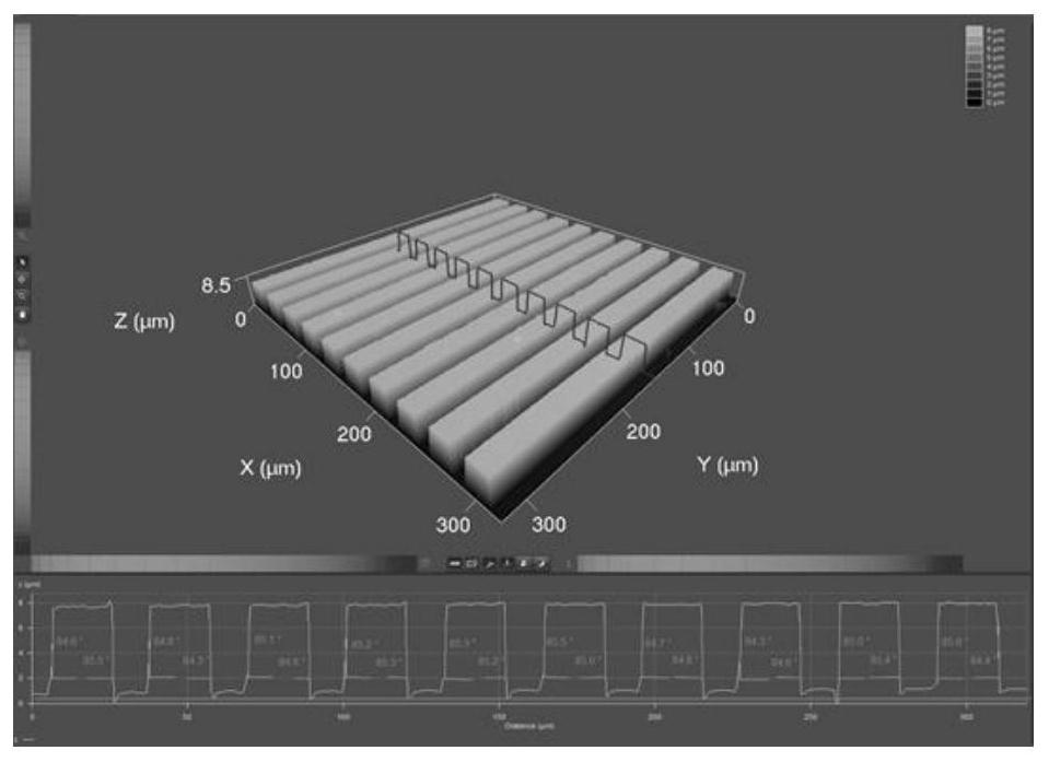
[0053] Example 1: For the reconstructed scanned graphics, such as Figure 7 As shown, select 10 sampling areas at different positions on the same waveguide or structural channel to analyze the roughness of the side wall, that is, m=1, n=10, and obtain the peak value, deep valley, and total value of each subdivided sampling area. height, and then average the waveguide sidewall roughness shown in Table 1 for all selected locations.

[0054] n PSp(μm) PSv(μm) PSt(μm) 1 0.205 0.232 0.437 2 0.289 0.183 0.472 3 0.29 0.365 0.655 4 0.232 0.292 0.525 5 0.301 0.262 0.563 6 0.273 0.144 0.416 7 0.291 0.243 0.534 8 0.485 0.171 0.656 9 0.35 0.187 0.537 10 0.348 0.144 0.492 AVG 0.3064 0.2223 0.5287

[0055] Table 1

Embodiment 2

[0056] Example 2: For the reconstructed scanned graphics, such as Figure 8 As shown, select multiple waveguide or structure channels, select a waveguide transverse area and conduct subdivided sampling analysis of this area in 10 areas, that is, m=10, n=10, and then calculate for all waveguide channels or structures average value. As shown in table 2.

[0057] m PSp(μm) PSv(μm) PSt(μm) 1 0.403 0.127 0.53 2 0.568 0.144 0.712 3 0.549 0.122 0.671 4 0.475 0.18 0.655 5 0.566 0.109 0.675 6 0.455 0.122 0.576 7 0.523 0.179 0.701 8 0.492 0.122 0.614 9 0.489 0.081 0.57 10 0.522 0.101 0.623 AVG 0.5042 0.1287 0.6327

[0058] Table 2


PUM


Abstract

The method of using the confocal laser scanning microscope system to measure the surface roughness of the medium involves the field of precision processing and precise measurement. The method includes designing the confocal laser scanning microscope system and setting an adjustable pinhole diaphragm in front of the detector; designing the The scanning range is 100 microns, the laser scanner with a control accuracy of 10 nanometers and the stage with adjustable object distance and inclination angle are selected. The laser with a wavelength of 405 nanometers is selected; the aperture pinhole is set to a value of <1.0 Airy unit, After selecting the scanning range and scanning layer thickness, scan and store the data; reconstruct the scanning image, select a shape curve in the plane, and give the average value of the peak roughness and total roughness of the shape curve; obtain multiple The average value of the peak roughness and the total roughness of the sampling length; the average value of the peak roughness and the total roughness is obtained by measuring the surface roughness of multiple waveguides with multiple sampling lengths; this method can be used in the production of large-scale micro-nano structures Non-destructive online fast detection in .

Description

technical field [0001] The invention relates to the field of precision processing and precise measurement of micro-nano-scale optical media devices and structures, in particular to a method for measuring the surface roughness of a medium by using a confocal laser scanning microscope system. Background technique [0002] Modern micro-nano-level processing has covered almost all fields, and the rapid growth is biomedical and micro-photonics and optoelectronics industries. In the field of micro-photonics and optoelectronics, the micro-nano-scale structure of dielectric materials is all the technologies, including the most mature planar lightwave circuit (PLC) technology, especially in the past ten years, silicon-based waveguide The research and widespread application of photonic devices has formed a new field of silicon-based integrated photonics. In recent years, with the development and promotion of silicon-based photonics integrated devices and systems, the current micro-na...

Claims


Application Information

Patent Timeline
Patent Type & Authority Patents(China)
IPC IPC(8): G01N21/84G01B11/30
Inventor 孙德贵尚鸿鹏形文超孙喆禹
Owner CHANGCHUN UNIV OF SCI & TECH
Why Eureka
Try Eureka