III-group nitride layer on silicon substrate

A nitride layer and silicon substrate technology, applied in the field of semiconductors, can solve problems such as restricting the performance of group III nitride semiconductor devices, and achieve the effects of large bond strength, improved performance, and strong fracture toughness

Pending Publication Date: 2019-06-14
JIANGXI ZHAO CHI SEMICON CO LTD
View PDF5 Cites 0 Cited by
  • Summary
  • Abstract
  • Description
  • Claims
  • Application Information

AI Technical Summary

Problems solved by technology

However, the thickness of the crack-free III-nitride layer obtained by the above method is still only 1~4um, which is still thinner than the ideal thickness of the III-nitride semiconductor device, thus restricting the silicon substrate to a certain extent. The performance of III-nitride semiconductor devices on

Method used


Image

  • III-group nitride layer on silicon substrate
  • III-group nitride layer on silicon substrate
  • III-group nitride layer on silicon substrate

Examples


Embodiment 1

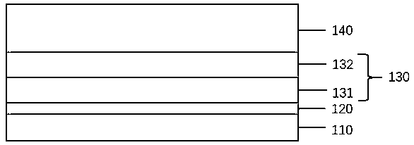
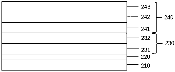
[0021] Embodiment 1, as figure 2 As shown, the present invention takes the III-nitride functional layer 240 to realize a light-emitting diode device as an example. The implementation provides a III-nitride layer on a silicon substrate, including III Group III nitride buffer layer 220, Group III nitride bottom layer 230 and Group III nitride functional layer 240, the Group III nitride bottom layer 230 includes an intermediate layer 231 and a base layer 232, and the intermediate layer 231 is B 0.1 al 0.9 N layer, the base layer 232 is a GaN layer, and the group III nitride functional layer 240 sequentially includes an n-type GaN layer 241 , a multi-quantum well layer 242 and a p-type GaN layer 243 to realize a light emitting diode device.

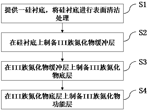
[0022] Such as image 3 Shown is a schematic diagram of the preparation method in the embodiment of the present invention, and the specific preparation process is as follows:

[0023] Step S1: provide a silicon substrate 210, the silicon ...


PUM

PropertyMeasurementUnit
thicknessaaaaaaaaaa

Abstract

The invention discloses an III-group nitride layer on a silicon substrate. The III-group nitride layer comprises a silicon substrate, and an III-group nitride buffer layer, an III-group nitride bottomlayer and an III-group nitride functional layer which are arranged on the silicon substrate in sequence, wherein the III-group nitride bottom layer comprises a middle layer and a substrate layer; themiddle layer comprises the components of BxAlyGa1-x-yN, wherein x is greater than or equal to 0.05 and less than or equal to 1, y is greater than or equal to 0 and less than or equal to 1, and x+ y is greater than or equal to 0 and less than or equal to 1; and the substrate layer comprises the components of AlzGa1-zN, wherein z is greater than or equal to 0 and less than or equal to 1. The III-group nitride layer has the following advantages that compared with a traditional AlGaN middle layer which is used when the III-group nitride layer grows on a silicon substrate, due to the fact that theB-N bond has higher bond strength and stronger fracture toughness than Al-N bond, more compressive stress can be accumulated in the growth process of the invention, the III-group nitride layer with alarger critical fracture thickness can be realized, and the performance of the III-group nitride semiconductor device is further improved.

Description

technical field [0001] The invention relates to the technical field of semiconductors, in particular to a group III nitride layer on a silicon substrate. Background technique [0002] Group III nitride materials have broad application prospects in many fields. For example, blue light-emitting diodes (LEDs) made of InGaN-based materials can realize high-efficiency and high-reliability solid-state lighting, and have rapidly achieved industrialization. High electron mobility transistors (HEMTs) made of AlGaN-based materials can work at extremely high frequencies and have also attracted extensive attention from researchers. At present, the vast majority of Group III nitride materials are realized by epitaxial growth on heterogeneous substrates. Commonly used heterogeneous substrates include sapphire substrates, silicon carbide substrates and silicon substrates. Each of these three substrates has its own advantages and disadvantages. Among them, silicon substrates have great pot...

Claims


Application Information

Patent Timeline
Patent Type & Authority Applications(China)
IPC IPC(8): H01L29/20H01L29/778H01L31/0304H01L31/101H01L33/32H01S5/30
Inventor 顾伟
Owner JIANGXI ZHAO CHI SEMICON CO LTD
Why Eureka
Try Eureka